Dual-energy electron flooding for neutralization of charged substrate

Active Publication Date: 2005-08-16
KLA TENCOR CORP
View PDF11 Cites 26 Cited by
  • Summary
  • Abstract
  • Description
  • Claims
  • Application Information

AI Technical Summary

Benefits of technology

[0014]One embodiment of the invention relates to a method of electron beam inspection or review of a substrate having insulating materials therein. An area of the substra

Problems solved by technology

However, as device design rules further shrink, and new processes (such as, for example, high aspect ratio (HAR) contacts in front-end-of-line (FEOL), HAR vias in back-end-of-line (BEOL), and dual damascene copper processes) are being widely implemented, it becomes more challenging to detect defects in device structures with smaller design rules and higher aspect ratios.
Further, image contrast variation caused by uneven charge distribution can make e-beam inspection unstable or un-inspectable.
Although conventional electron microscopy systems and techniques typically produce images having an adequate level of quality under some conditions, they produce poor quality images of the sample for some appl

Method used


Image

  • Dual-energy electron flooding for neutralization of charged substrate
  • Dual-energy electron flooding for neutralization of charged substrate
  • Dual-energy electron flooding for neutralization of charged substrate

Examples


Embodiment Construction

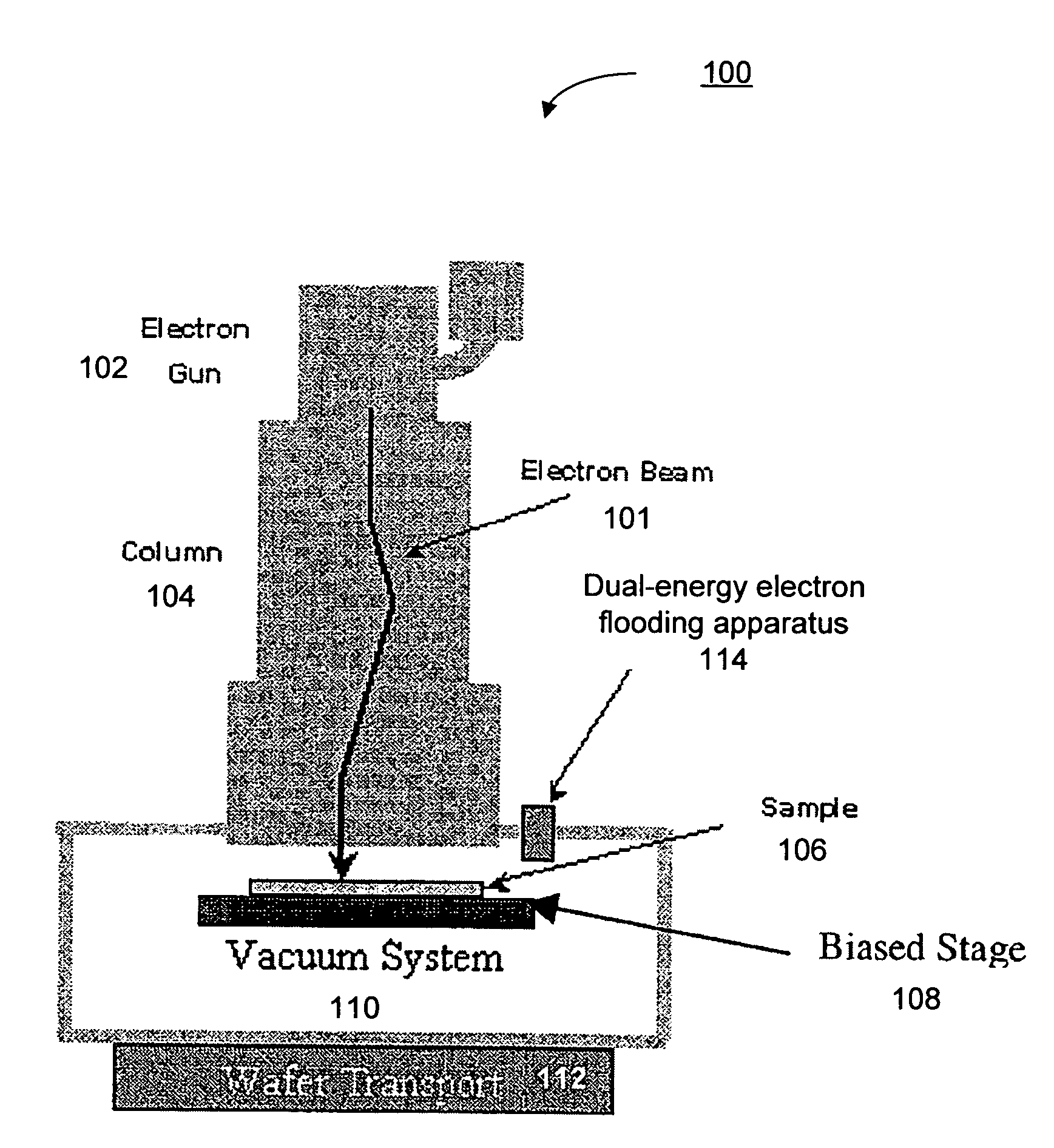
[0016]FIG. 1 is a schematic diagram of an electron beam inspection system 100 in accordance with an embodiment of the invention. The e-beam system 100 generates and directs an incident electron beam 101 towards an area of interest on a sample or specimen 106 for use in generating an image of the area.

[0017]As shown in FIG. 1, the incident beam 101 may be generated by an electron gun 102. A column 104 including various components in a vacuum is used to direct the electron beam 101 towards the surface of the sample 106. The column 104 typically includes various electron lenses, apertures, and other components.

[0018]The sample 106 may be held on a stage 108. The stage 106 may be biased at a controllable electrical potential. Like the column 104, because the incident beam comprises electrons, a vacuum system 110 is used to pump the chamber containing the sample 106 and stage 108 (as well as the column 104). The sample 106 may comprise, for example, a wafer or other substrate. A wafer tr...


PUM


Abstract

One embodiment disclosed relates to a method of electron beam inspection or review of a substrate having insulating materials therein. An area of the substrate is simultaneously exposed to a lower-energy electron beam and an overlapping higher-energy electron beam. The area is subsequently inspected with another electron beam. Another embodiment disclosed relates to an electron beam tool for examination of a substrate having insulating materials therein. A first cathode is configured as an electron source for a lower-energy electron beam, and a second cathode is configured as an electron source for a higher-energy electron beam. At least one electron lens is configured to focus the lower-energy electron beam and the higher-energy electron beam onto an overlapping area of a substrate. An electron beam column is subsequently used to examine the substrate.

Description

BACKGROUND OF THE INVENTION[0001]1. Field of the Invention[0002]The present invention relates generally to specimen inspection and review. More particularly, the present invention relates to electron beam inspection and review systems.[0003]2. Description of the Background Art[0004]Automated inspection and review systems are important in process control and yield management for the semiconductor and related microelectronics industries. Such systems include optical and electron beam (e-beam) based systems.[0005]In the manufacture of semiconductor devices, detection of physical defects and electrical failure earlier in the fabrication process is becoming increasingly important to shorten product development cycles and increase product yield and productivity. Advanced wafer inspection systems based on scanning electron microscopy technology have been used to detect defects and electrical failure as voltage contrast defects. However, as device design rules further shrink, and new proces...

Claims


Application Information

Patent Timeline
IPC IPC(8): G01N23/225G01N23/22H01J37/26G01Q30/02H01J37/02
CPCG01N23/225H01J37/026H01J2237/0041H01J2237/2817
Inventor MANKOS, MARIANPARKER, DONALD J.
Owner KLA TENCOR CORP
Why Eureka
Try Eureka