Calcium doped polysilicon gate electrodes

a polysilicon gate electrode and calcium doped technology, applied in the field of pchannel mos field effect transistors, can solve the problems of exacerbate the poly depletion effect, the reduction is not usually sufficient for very thin gate oxides, and the change of the properties of the substrate is not wanted, so as to reduce the migration of boron dopant, improve the activation of boron dopant, and reduce the problem of boron penetration

Inactive Publication Date: 2005-08-16
BELL SEMICON LLC
View PDF7 Cites 10 Cited by
  • Summary
  • Abstract
  • Description
  • Claims
  • Application Information

AI Technical Summary

Benefits of technology

[0006]The present invention provides calcium doped polysilicon gate electrodes for PMOS containing semiconductor devices. The calcium doped PMOS gate electrodes reduce migration of the boron dopant out of the gate electrode, through the gate dielectric and into the substrate thereby reducing boron penetration problem increasingly encountered with smaller device size regimes and their thinner gate dielectrics. Calcium doping of the gate electrode may be achieved by a variety of techniques. It is further believed that the calcium doping may improve the boron dopant activation in the gate electrode, thereby further improving performance by reducing the poly depletion effect.

Problems solved by technology

The scaled-down gate dielectric has become so thin that boron, which is traditionally used to dope the gate electrode for P-channel MOS field effect transistors, can migrate from the gate electrode through the thin gate dielectric and penetrate into the underlying semiconductor substrate, causing unwanted changes in the properties of the substrate.
However, that reduction is not usually sufficient for very thin gate oxides, and in addition it may even exacerbate the poly depletion effect.
However, these approaches have substantial drawbacks in that determining the right work function for such gate electrodes that is suitable for either of N or P channel devices (necessary for CMOS devices) is difficult.
In addition, the interface of these materials with common gate dielectric materials, such as SiO2, is not nearly so well understood as the silicon (including polysilicon) and gate oxide interface, so the stability of these materials on a gate dielectric is an issue.

Method used


Image

  • Calcium doped polysilicon gate electrodes
  • Calcium doped polysilicon gate electrodes
  • Calcium doped polysilicon gate electrodes

Examples


Embodiment Construction

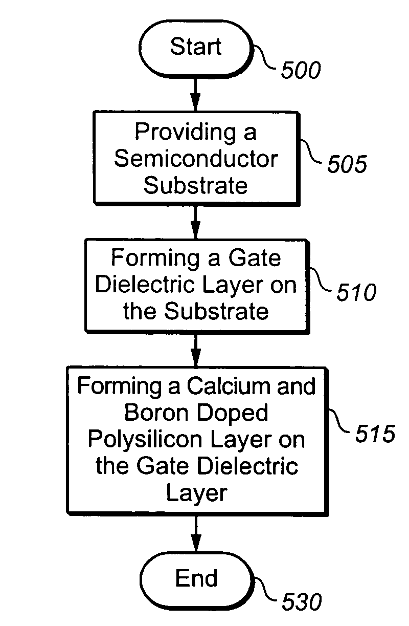
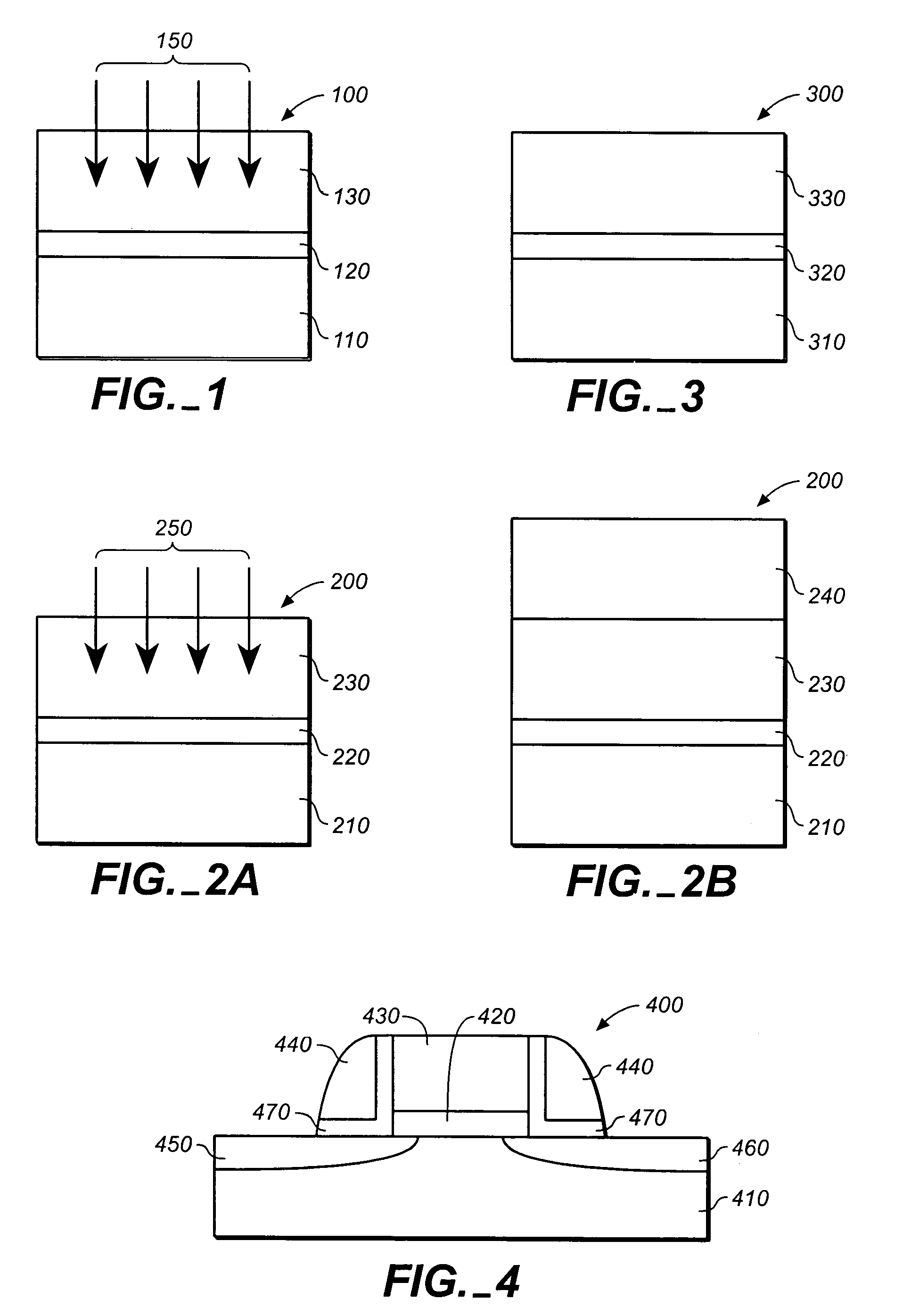
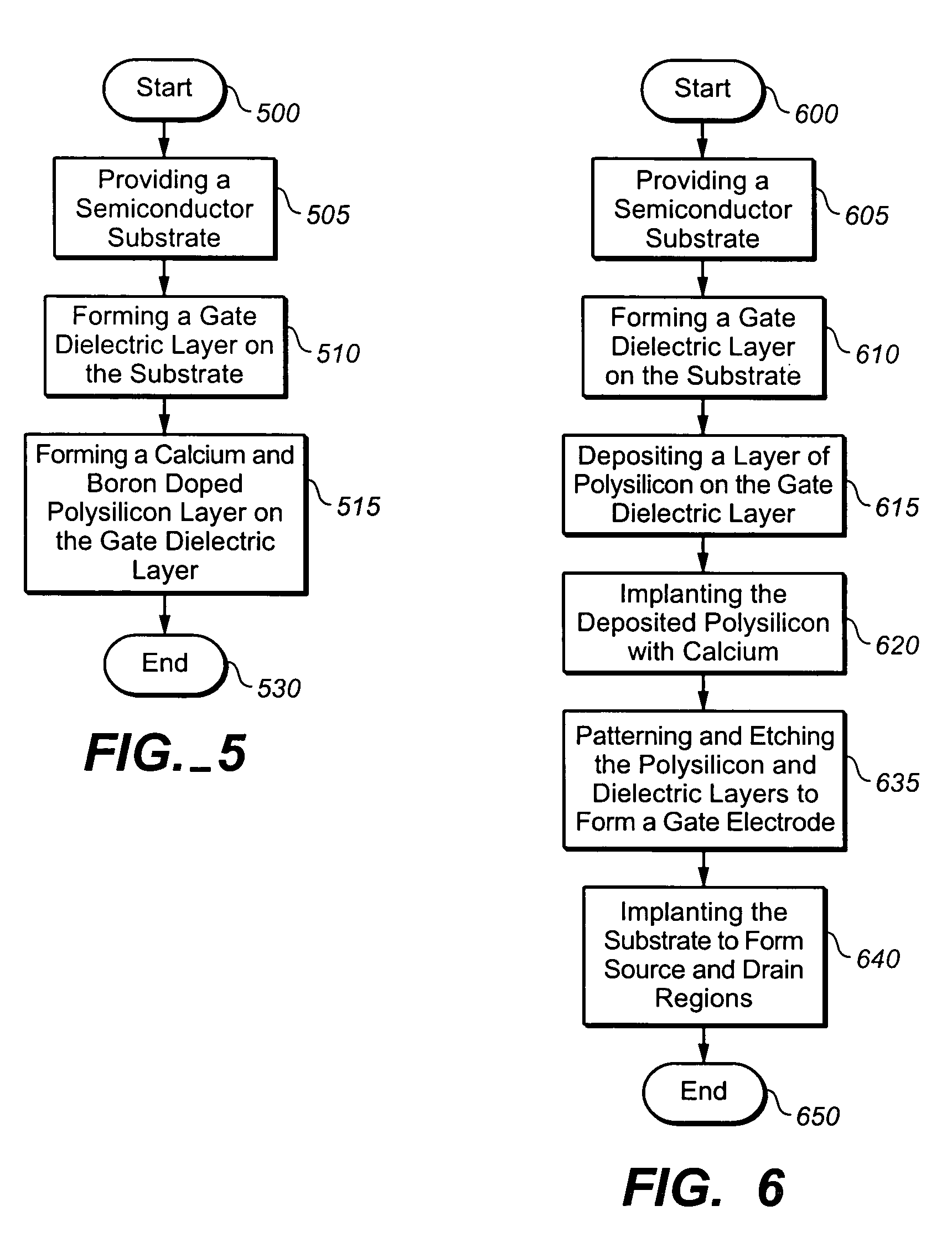
[0018]While the present invention will be described with reference to a few specific embodiments, the description is illustrative of the invention and not to be construed as limiting the invention. Various modifications to the present invention can be made to the preferred embodiments by those skilled in the art without departing from the true spirit and scope of the invention as defined by the appended claims. The present invention relates to a semiconductor device and several methods for creating that semiconductor device. In the described embodiments of the invention, a gate electrode for a P-channel MOSFET, wherein calcium has been added to a polysilicon layer that has been applied over a gate dielectric layer during device fabrication. This calcium may be incorporated into the polysilicon in a variety of ways including implantation to dope a deposited polysilicon gate electrode material, deposition of a calcium doped polysilicon gate electrode material, for example, by chemical...


PUM

PropertyMeasurementUnit
energyaaaaaaaaaa
sizesaaaaaaaaaa
thicknessaaaaaaaaaa

Abstract

A calcium doped polysilicon gate electrodes for PMOS containing semiconductor devices. The calcium doped PMOS gate electrodes reduce migration of the boron dopant out of the gate electrode, through the gate dielectric and into the substrate thereby reducing the boron penetration problem increasingly encountered with smaller device size regimes and their thinner gate dielectrics. Calcium doping of the gate electrode may be achieved by a variety of techniques. It is further believed that the calcium doping may improve the boron dopant activation in the gate electrode, thereby further improving performance.

Description

FIELD OF THE INVENTION[0001]The present invention relates generally to P-channel MOS field effect transistors (MOSFETs), and more particularly, to preventing boron penetration from the gate electrode in a MOSFET and with the effect of preventing poly depletion in the gate electrode.BACKGROUND OF THE INVENTION[0002]As CMOS manufacturing technology achieves smaller feature sizes, for example, 01. microns and below, there has been a corresponding scaling down of the gate dielectric. The scaled-down gate dielectric has become so thin that boron, which is traditionally used to dope the gate electrode for P-channel MOS field effect transistors, can migrate from the gate electrode through the thin gate dielectric and penetrate into the underlying semiconductor substrate, causing unwanted changes in the properties of the substrate.[0003]Boron penetration may be reduced by incorporating nitrogen in the gate dielectric or polysilicon gate. However, that reduction is not usually sufficient for...

Claims


Application Information

Patent Timeline
Patent Type & Authority Patents(United States)
IPC IPC(8): H01L21/02H01L29/76H01L21/336H01L29/66H01L21/265H01L21/28H01L29/49H01L29/78
CPCH01L21/265H01L21/28035H01L29/4925H01L29/6656H01L29/78
Inventor MIRABEDINI, MOHAMMAD R.SUN, GRACE S.ARONOWITZ, SHELDON
Owner BELL SEMICON LLC
Why Eureka
Try Eureka