Spatial light modulator, spatial light modulator array, image forming device and flat panel display

a technology array, which is applied in the direction of static indicating devices, instruments, optical elements, etc., can solve the problems of inability to perform high-speed return, increase and the inability to realize the reduction of operating voltage simultaneously. , to achieve the effect of reducing the operating voltage and increasing the on/off switching speed of spatial light modulator

Inactive Publication Date: 2005-08-16
FUJIFILM CORP +1
View PDF4 Cites 97 Cited by
  • Summary
  • Abstract
  • Description
  • Claims
  • Application Information

AI Technical Summary

Benefits of technology

[0015]It is an object of the invention to provide a spatial light modulator, a spatial light modulator array, an image forming device and a flat panel display which can solve the problem discussed above, and in which both the reduction in the operating voltage, and the increase of the ON / OFF switching speed of the spatial light modulator can be simultaneously realized.

Problems solved by technology

However, a spatial light modulator in the related art in which the returning of the movable thin film 9 to the initial state depends on the elastic restoring force of the elastic layer 12 constituting the movable thin film 9 as described above has a problem in that it is impossible to simultaneously realize the reduction in the operating voltage, and the increase of the ON / OFF switching speed of the spatial light modulator.
By contrast, in the case where the elastic restoring force is weak, when the applied voltage is canceled, the returning operation is slow, thereby causing a problem in that high-speed returning cannot be performed.

Method used


Image

  • Spatial light modulator, spatial light modulator array, image forming device and flat panel display
  • Spatial light modulator, spatial light modulator array, image forming device and flat panel display
  • Spatial light modulator, spatial light modulator array, image forming device and flat panel display

Examples


second embodiment

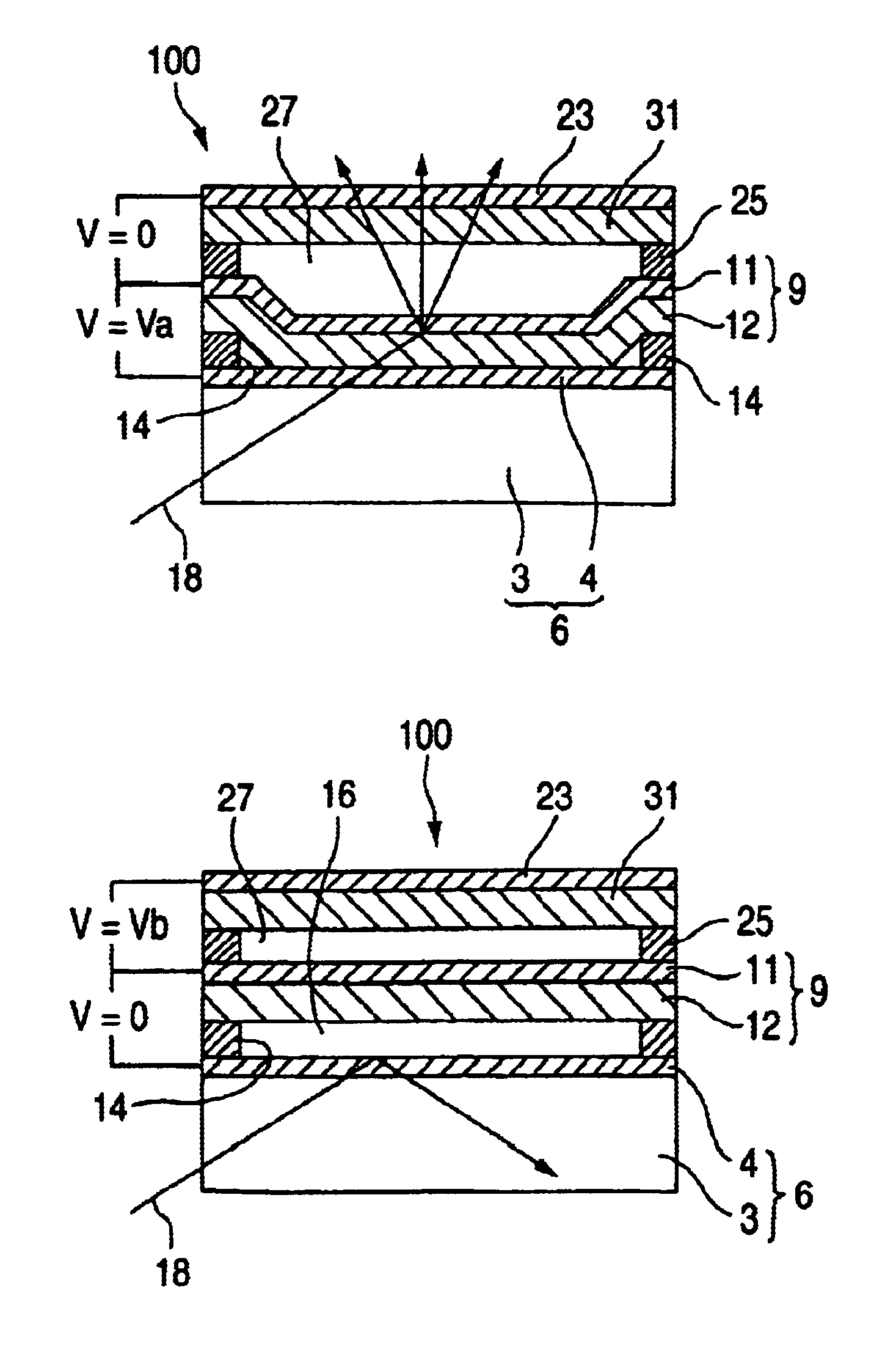
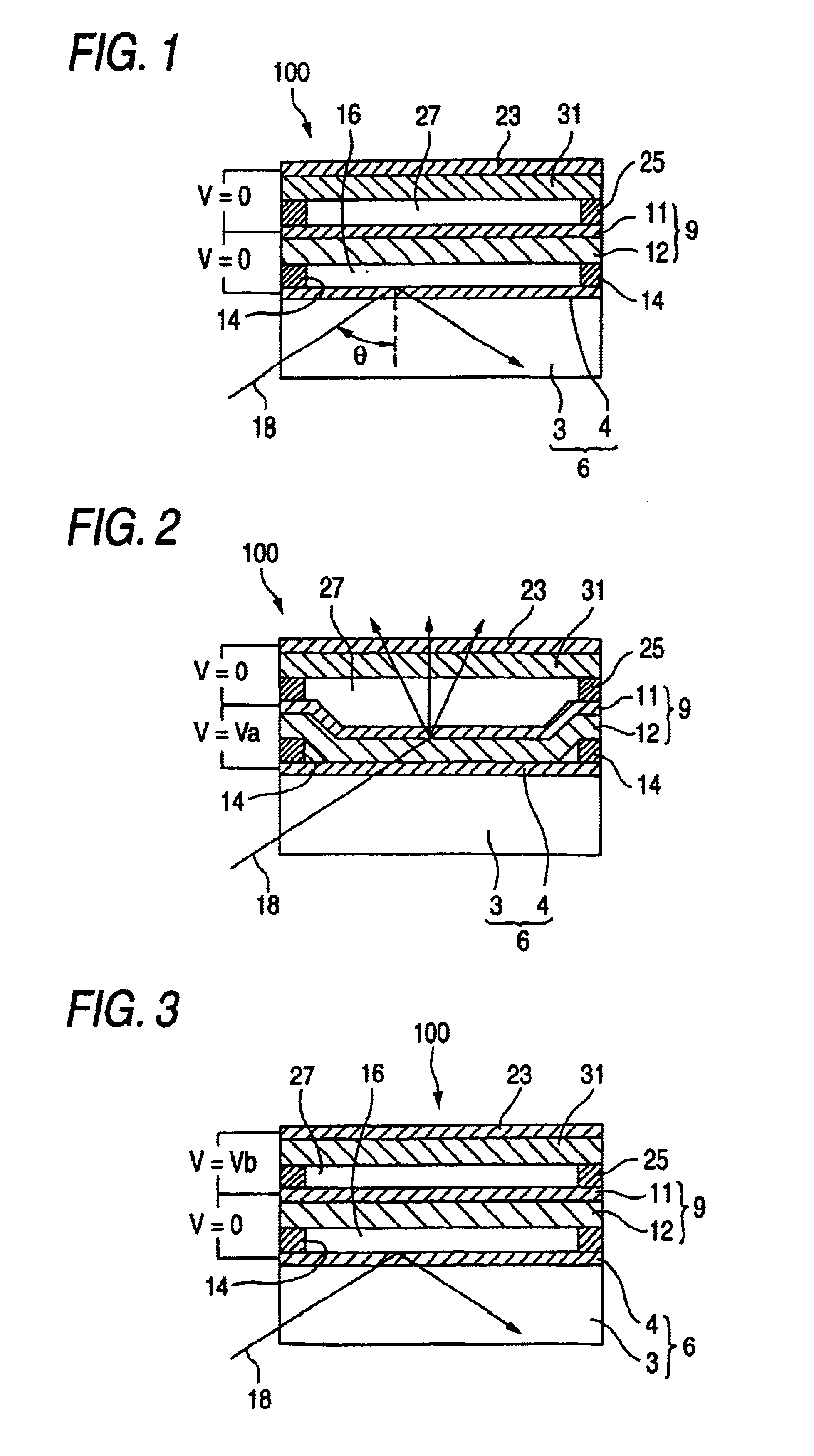
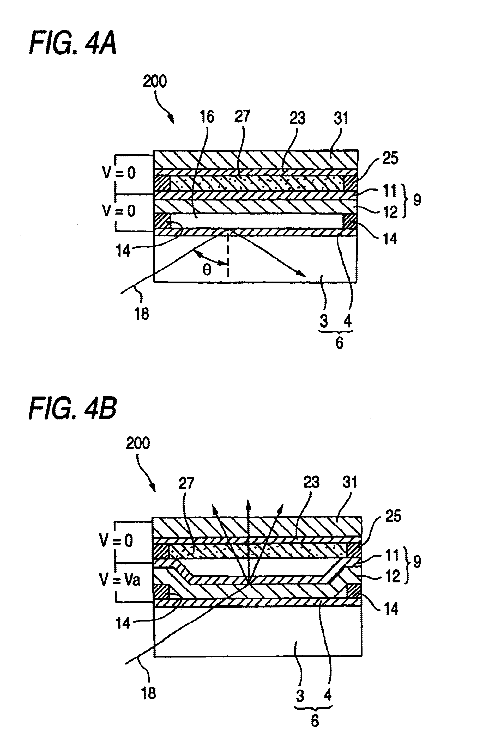
[0060]Next, the spatial light modulator of the invention will be described.

[0061]FIGS. 4A and 4B are section views showing the configuration of the spatial light modulator of the embodiment.

[0062]In the spatial light modulator 200 of the embodiment, the gap between the movable thin film 9 and the returning electrode 23 is filled with a transparent spacer 27.

[0063]The transparent spacer 27 is disposed so as to fill the gap which is formed between the movable thin film 9 and the restoring electrode 23 by the support 25 in the non-driven state of the spatial light modulator 200. When the movable thin film 9 is returned toward the returning electrode 23 in the OFF state of the spatial light modulator, the spacer prevents the movable thin film from being excessively flexurally deformed toward the returning electrode 23.

[0064]As the spacer 27, useful is a material which has a predetermined insulating performance, such as silicon oxide, silicon nitride, ceramics, or a resin.

[0065]In the th...

third embodiment

[0066]Next, the spatial light modulator of the invention will be described.

[0067]FIGS. 5 to 7 show the configuration of the spatial light modulator of the embodiment. FIG. 5 is a view showing the OFF state of the spatial light modulator, FIG. 6 is a view showing the ON state of the spatial light modulator, and FIG. 7 is a view showing a state change of the spatial light modulator from the ON state to the OFF state.

[0068]As shown in FIGS. 5 to 7, the spatial light modulator 300 of the embodiment comprises: a support substrate 6 in which a transparent electrode layer 4 is stacked on a transparent substrate 13; a movable thin film 9 which has a stacked structure of an electrode layer 11 and an elastic layer 12, which is transparent, and which is placed above the support substrate 6 via a support 14 to be opposed to the support substrate with being separated by a predetermined gap distance in a manner that the film is flexurally deformable toward the support substrate 6; a transparent r...

first embodiment

[0078]When the spatial light modulator 300 is to be switched from the ON state shown in FIG. 6 to the OFF state, the voltage application between the electrode layers 4 and 11 of the support substrate 6 and the movable thin film 9 is canceled, and the predetermined driving voltage Vb is simultaneously applied between the electrode layer 11 of the movable thin film 9 and the returning electrode 23, thereby causing the movable thin film 9 to be returned at a higher speed from the flexural deformation. This is identical with the first embodiment described above.

[0079]The light modulating operation by the spatial light modulator 300 will be described in detail. FIG. 8 is a graph showing the emission spectrum of the light 48 incident on the support substrate 6. The incident light 48 is light having a center wavelength λ0 of about 360 nm.

[0080]In the spatial light modulator 300 of the embodiment, for example, the gap distances tON and tOFF between the dielectric multilayer film mirrors 43 ...


PUM

PropertyMeasurementUnit
tensile stressaaaaaaaaaa
refractive indexaaaaaaaaaa

Abstract

A spatial light modulator has: a support substrate that has an electrode layer; and a movable thin film that has at least an electrode layer, and that is opposingly placed above the support substrate with being separated by a predetermined gap distance in a manner that the movable thin film is flexurally deformable toward the support substrate, and in which a predetermined driving voltage is applied between the electrode layer of the support substrate and the electrode layer of the movable thin film to cause the movable thin film to be deflected toward the support substrate by an electrostatic force acting between the electrode layers. A returning electrode is disposed on an side of the movable thin film opposite to the side which is opposed to the support substrate to apply an electrostatic force of attracting the movable thin film when a driving voltage is applied.

Description

BACKGROUND OF THE INVENTION[0001]1. Field of the Invention[0002]The present invention relates to a spatial light modulator, a spatial light modulator array, an image forming device and a flat panel display which perform light modulation by applying a predetermined voltage between an electrode layer of a support substrate and that of a movable thin film opposed to the support substrate to flexurally displace the movable thin film.[0003]2. Description of the Related Art[0004]FIGS. 15 and 16 show an example of a spatial light modulator in the related art which is produced by a micromachining process including steps of film growth, photolithography, and etching of a sacrifice layer (a later which is to be removed away later in order to form a gap), and in which the light transmittance is changed by an electromechanical operation.[0005]In the spatial light modulator 1, a transparent electrode layer 4 is stacked on an optical waveguide 3 to form a support substrate 6, and a movable thin f...

Claims


Application Information

Patent Timeline
Patent Type & Authority Patents(United States)
IPC IPC(8): G02B26/02G02B6/35
CPCG02B26/001G02B26/02G02B6/3524G02B6/357
Inventor MOCHIZUKI, FUMIHIKO
Owner FUJIFILM CORP
Why Eureka
Try Eureka