Reading circuit, reference circuit, and semiconductor memory device

a reading circuit and reference circuit technology, applied in the direction of static storage, digital storage, instruments, etc., can solve the problems of inability to easily perform data read at high speed, undesirably prolong the read time, and difficult to obtain a sufficiently large operation margin, so as to increase the reading operation margin and increase the reading speed

Active Publication Date: 2005-08-16
SAMSUNG ELECTRONICS CO LTD
View PDF4 Cites 27 Cited by
  • Summary
  • Abstract
  • Description
  • Claims
  • Application Information

AI Technical Summary

Benefits of technology

[0130]An appropriate reference element can easily be obtained as follows. An element having the same structure as that of the memory cell is used, and the threshold thereof is adjusted such that the element has the same characteristics as those of the memory cell.
[0131]Thus, the invention described herein ma...

Problems solved by technology

In such a case where the current level difference between the cell current levels and the reference current levels is relatively small, it is not easy to obtain a sufficiently large operation margin, especially in a reading circuit.
This undesirably extends the read time.
Therefore, data read cannot be easily performed at high speed.
However, the parallel sensing system, which requires a plurality of sense amplifiers, is disadvantageous in, for example, increasing the area of the chip occupied by sense amplifiers and in increasing the level of current instantaneously consumed.
This makes it difficult to enlarge the absolute operation margin at each of the operating points of the sense amplifiers H5 through H7.
However, such a reading circuit has a lower sensing voltage c...

Method used


Image

  • Reading circuit, reference circuit, and semiconductor memory device
  • Reading circuit, reference circuit, and semiconductor memory device
  • Reading circuit, reference circuit, and semiconductor memory device

Examples


example 1

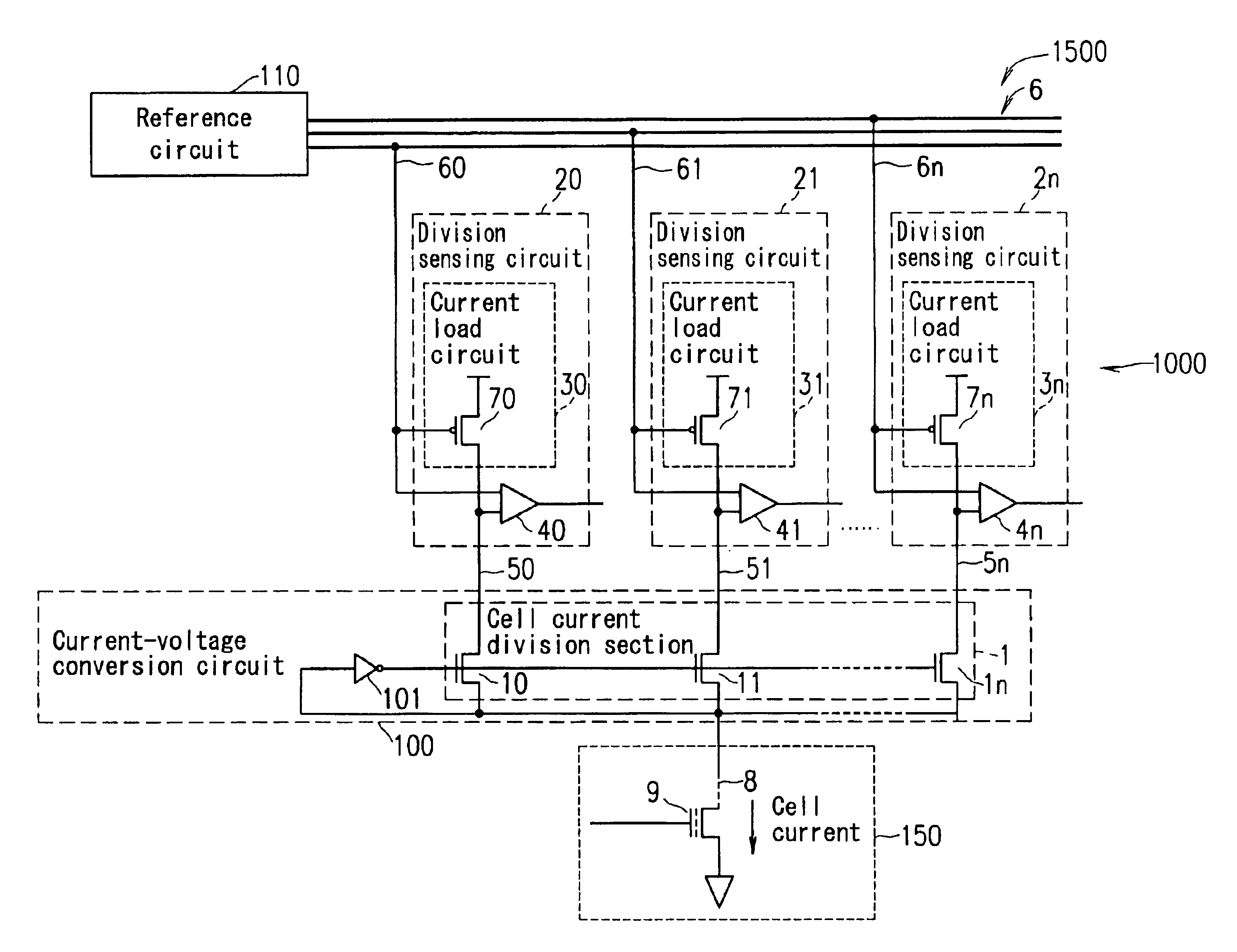
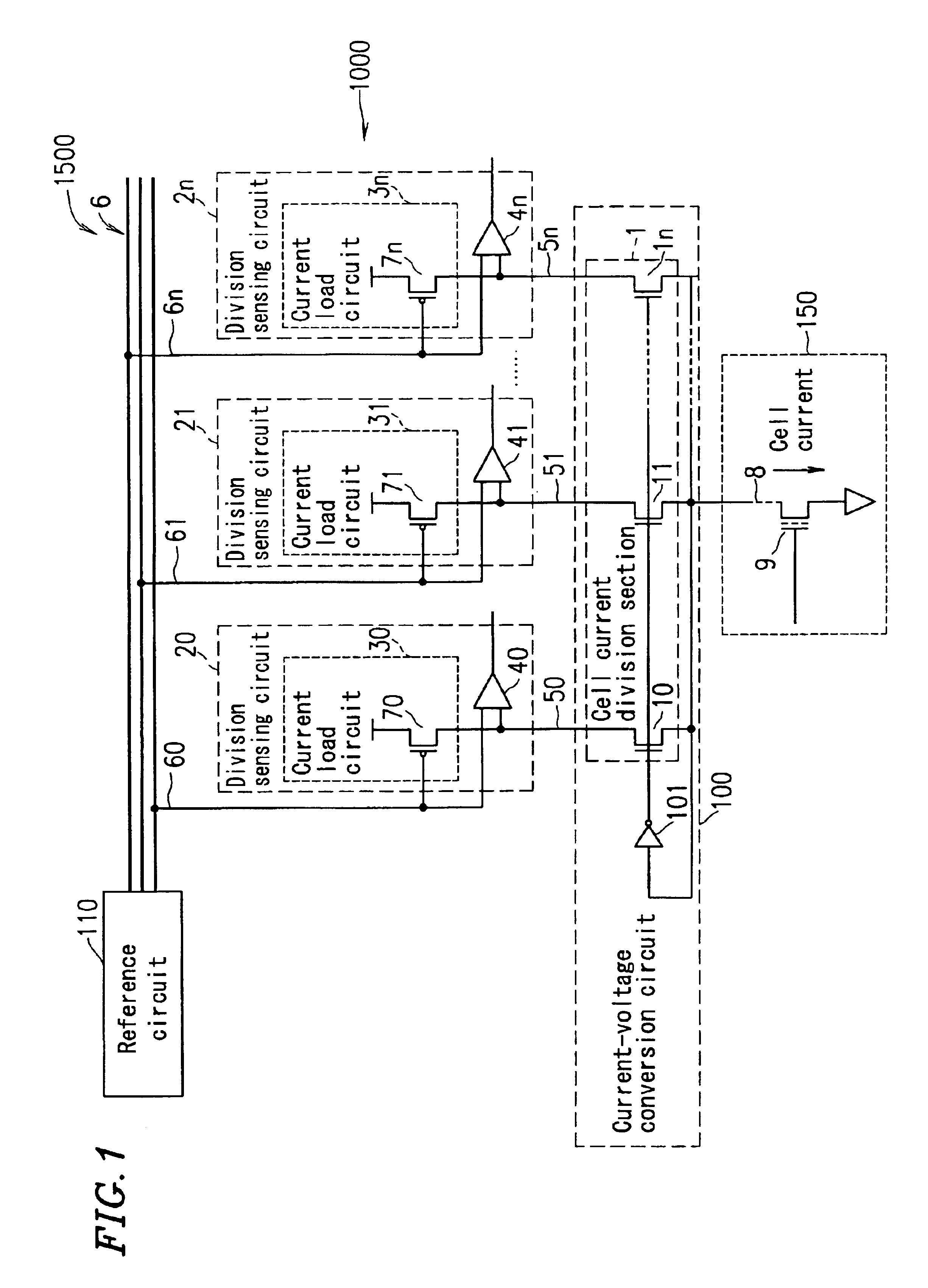
[0154]FIG. 1 is a schematic view of a semiconductor memory device 1500 according to a first example of the present invention.

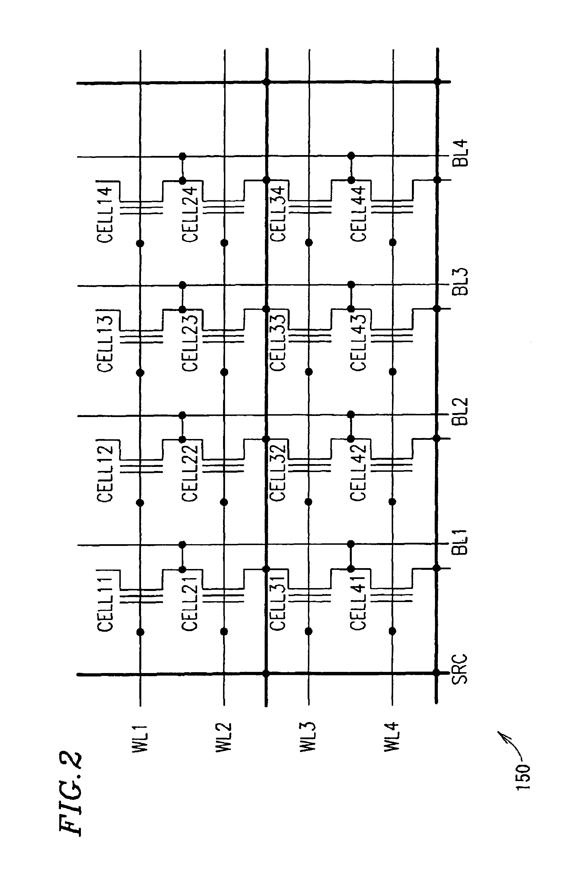
[0155]The semiconductor memory device 1500 includes a memory cell array 150 including a plurality of memory cells, a reading circuit 1000 for reading data from one of the plurality of memory cells, and a reference circuit 110 for generating a reference voltage for reading data.

[0156]In FIG. 1, the reading circuit 1000 is shown as reading data from only one memory cell. This is merely exemplary, and the reading circuit 1000 may read data from one selected memory cell 9 among the plurality of memory cells.

[0157]As shown in FIG. 1, the reading circuit 1000 supplies a cell current to the selected memory cell 9, among the plurality of memory cells, via a bit line 8 and converts the level of the cell current flowing through the memory cell 9 into a sensing voltage by current-voltage conversion. Then, the reading circuit 1000 compares the sensing voltage with a refer...

example 2

[0226]In the first example, no specific structure of the reference circuit was described. In a second example of the present invention, an exemplary structure of the reference circuit 110 will be described.

[0227]FIG. 4 shows a circuit configuration of the reference circuit 110 shown in FIG. 1.

[0228]As shown in FIG. 4, the reference circuit 110 includes a plurality of reference voltage setting circuits 110-0 through 110-n. In the second example, the number of the reference voltage setting circuits included in the reference circuit 110 is an integer of 2 or greater.

[0229]The reference voltage setting circuit 110-0 supplies a reference current to a selected reference element 9-r0 via a reference bit line 8-r0, and converts a reference current flowing through the reference element 9-r0 into a reference voltage.

[0230]The reference voltage setting circuit 110-1 supplies a reference current to a selected reference element 9-r1 via a reference bit line 8-r1, and converts a reference current...

example 3

[0284]In a third example of the present invention, a semiconductor memory device including two reference circuits will be described.

[0285]FIG. 5 schematically shows a structure of a semiconductor memory device 2500 according to the third example of the present invention.

[0286]The semiconductor memory device 2500 includes a memory cell array 150 including a plurality of memory cells, a reading circuit 2000 for reading data from one of the plurality of memory cells, and reference circuits 110 and 120 for generating a reference voltage used for reading data.

[0287]In the following description, elements having substantially the same functions as those in the first and second examples bear the same reference numerals, and the same functions will not be described.

[0288]The reading circuit 2000 includes a plurality of division sensing circuits 20 through 2n and a current-voltage conversion circuit 100.

[0289]The division sensing circuits 20 through 2n are each supplied with two types of refe...


PUM


Abstract

A reading circuit, for reading data from one memory cell of a plurality of memory cells, includes a plurality of division sensing circuits each connected to the one memory cell via a sensing line corresponding thereto among a plurality of sensing lines; and a current-voltage conversion circuit for converting a current flowing through each sensing line into a sensing voltage representing a potential of the corresponding sensing line. Each division sensing circuit includes a current load circuit for supplying a current to the one memory cell via a corresponding sensing line, and a sense amplifier for sensing a potential difference between the corresponding sensing line and a corresponding reference line of a plurality of reference lines. The current load circuit included in at least one division sensing circuit has a current supply capability different from that of the current load circuit included in another division sensing circuits.

Description

BACKGROUND OF THE INVENTION[0001]1. Field of the Invention[0002]The present invention relates to a reading circuit, a reference circuit, and a semiconductor memory device including such a reading circuit and such a reference circuit.[0003]2. Description of the Related Art[0004]In general, a reading circuit for reading data from a memory cell array including a plurality of memory cells supplies an electric current to a memory cell having data stored therein, and compares the current (cell current) flowing through the memory cell with a reference current so as to determine whether the level of the cell current is higher or lower than the level of the reference current. Thus, the data written in the memory cell is read. Such a system of reading data is referred to as a “current sensing system”.[0005]For example, data is read from so-called two-level memory cells which can store 1-bit data in one memory cell as described below with reference to FIG. 9B. A first state in which the level ...

Claims


Application Information

Patent Timeline
IPC IPC(8): G11C11/56G11C16/28G11C16/06G11C7/00G11C16/02G11C16/04
CPCG11C11/5642G11C16/28G11C2211/5634G11C7/00
Inventor MORI, YASUMICHIYOSHIMOTO, TAKAHIKOANZAI, SHINSUKENOJIMA, TAKESHI
Owner SAMSUNG ELECTRONICS CO LTD
Why Eureka
Try Eureka