Plasma display panel utilizing carbon nanotubes and method of manufacturing the front panel of the plasma display panel

a technology of plasma display panel and carbon nanotube, which is applied in the manufacture of electrode systems, electric discharge tubes/lamps, instruments, etc., can solve the problems of the display panel and the difficulty of technically growing carbon nanotubes on the mgo protective layer, and achieve the effects of improving the contrast ratio of the display screen, good secondary electron emission characteristic, and high-quality pictures

Inactive Publication Date: 2005-08-23
SAMSUNG SDI CO LTD
View PDF6 Cites 35 Cited by
  • Summary
  • Abstract
  • Description
  • Claims
  • Application Information

AI Technical Summary

Benefits of technology

[0019]Accordingly, the plasma display panel using carbon nanotubes having a good secondary electron emission characteristic improv

Problems solved by technology

Particularly, the plasma display panel of FIG. 2 has difficulty in

Method used


Image

  • Plasma display panel utilizing carbon nanotubes and method of manufacturing the front panel of the plasma display panel
  • Plasma display panel utilizing carbon nanotubes and method of manufacturing the front panel of the plasma display panel
  • Plasma display panel utilizing carbon nanotubes and method of manufacturing the front panel of the plasma display panel

Examples


first embodiment

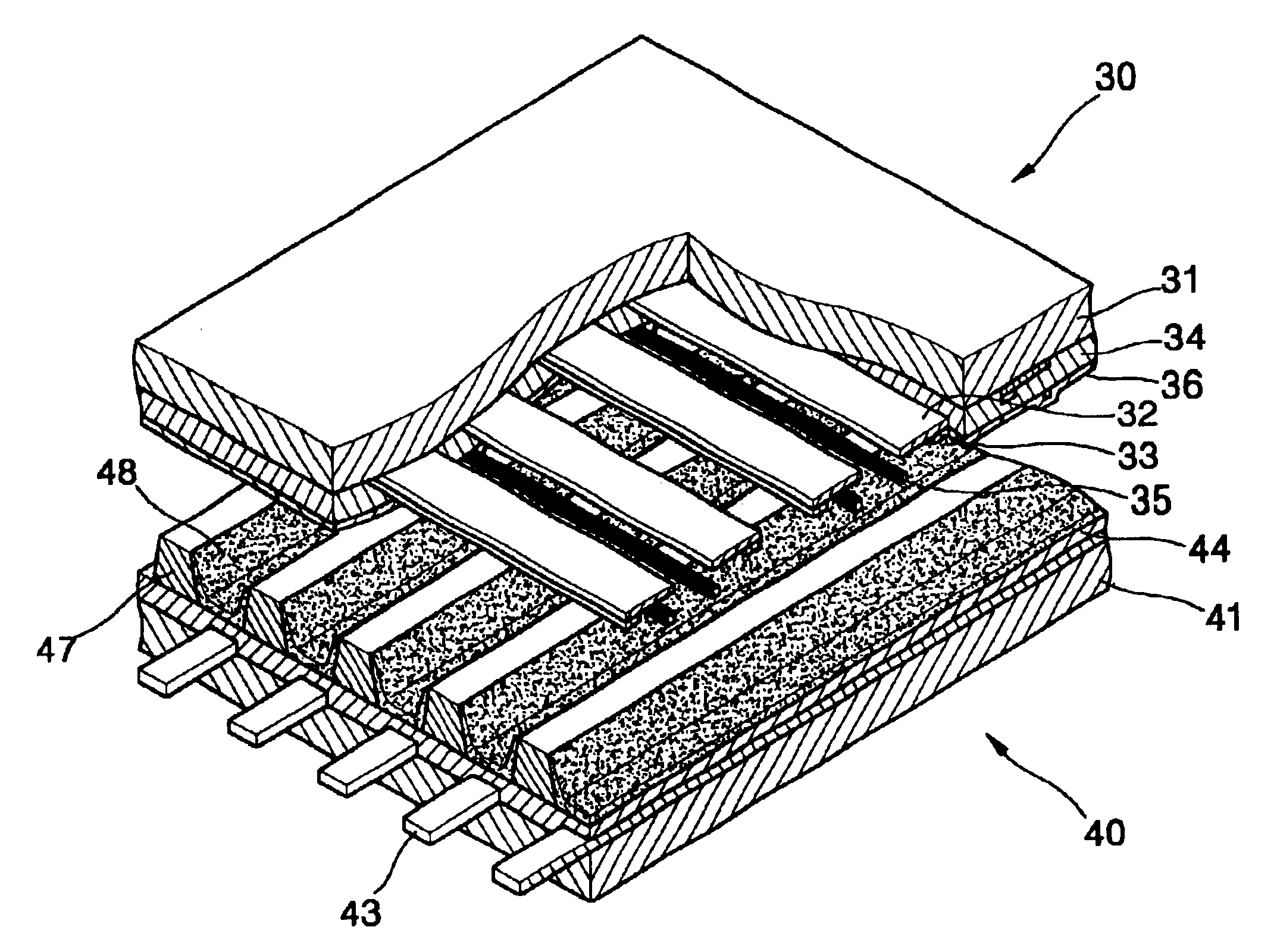
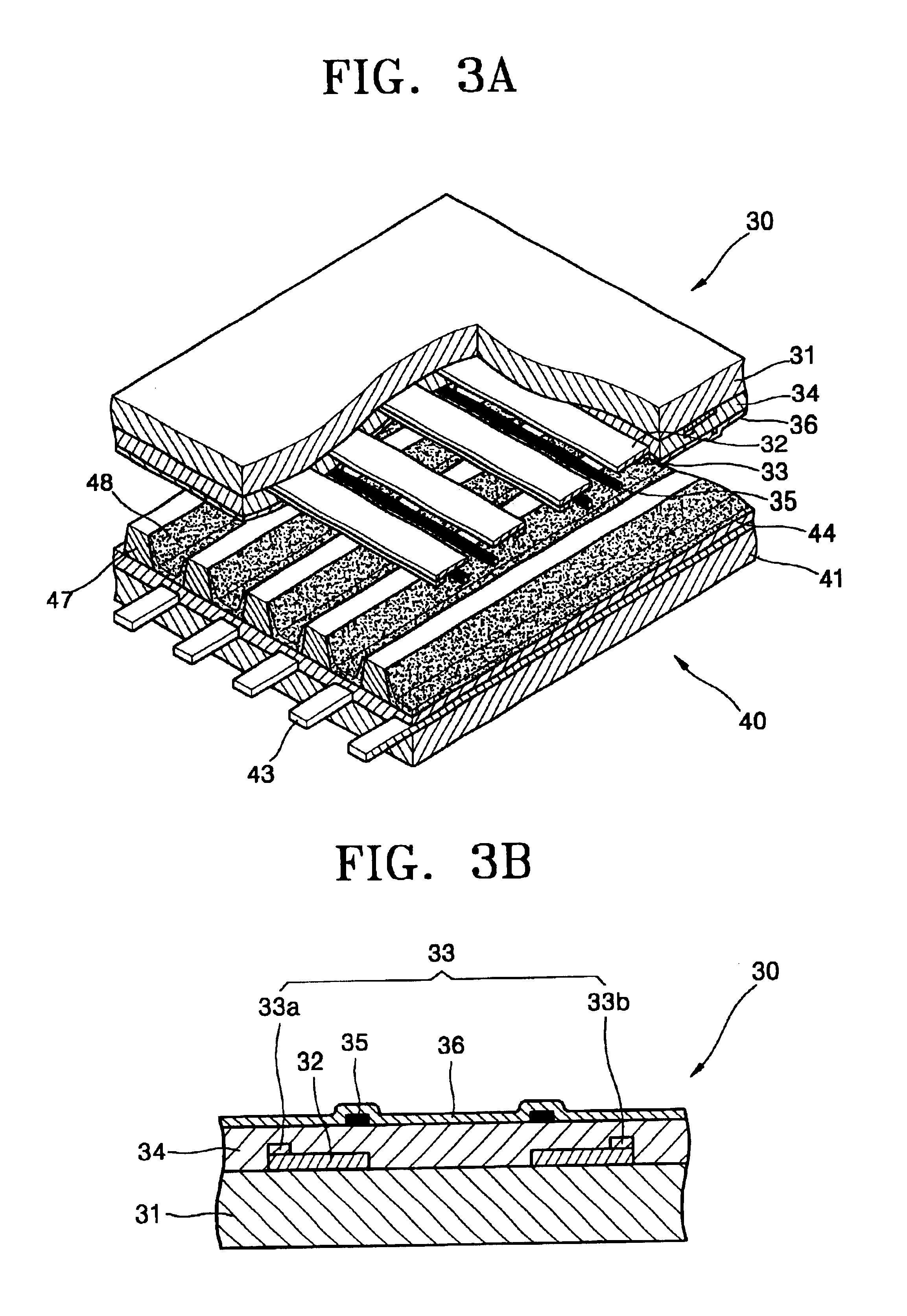
[0033]Referring to FIG. 3A, in a front panel 30 of the plasma display panel according to the present invention, transparent electrodes 32 are formed as strips on a glass substrate 31. Bus electrodes 33 are each formed as strips along the outer edge portion on each of the transparent electrodes 32. A dielectric layer 34 for covering the display electrodes 32 and the bus electrodes 33 is deposited on the glass substrate 31. Here, the bus electrodes 33 placed at the left side on the transparent electrodes 32 are referred to as scan electrodes 33a, and the bus electrodes 33 placed at the right side on the transparent electrodes 32 are referred to as sustain electrodes 33b.

[0034]Carbon nanotube strips 35 are aligned on the dielectric layer 34 such that they face the display electrodes 32. An MgO protective layer 36 is formed on the dielectric layer 34 while covering the carbon nanotube strips 35.

[0035]A rear panel 40 of the plasma display panel according to the first embodiment of the p...

second embodiment

[0041]FIG. 4A is an open-cut perspective view of a plasma display panel according to the present invention. FIG. 4B is a cross section of a plasma display panel according to a second embodiment of the present invention.

[0042]The plasma display panel according to the second embodiment of the present invention is the same as that according to the first embodiment of the present invention except that the carbon nanotube strips 35 are aligned directly over the scan electrodes 33a and the sustain electrodes 33b.

[0043]In the plasma display panels according to the first and second embodiments of the present invention, the carbon nanotube strips 35 are each about 70-100 μm wide, the bus electrodes 33 are each about 60 μm wide, and the transparent electrodes 32 are about 300 μm wide.

[0044]On one hand, the carbon nanotube strips 35 printed on the dielectric layer 34 improve the secondary electron emission characteristics of a plasma display panel on the whole. On the other hand, the opaquene...


PUM


Abstract

A plasma display panel using carbon nanotubes is provided. In the front panel of the plasma display panel, transparent electrodes are formed as strips on the glass substrate. Bus electrodes are each formed as strips along the outer edge on the upper surface of each of the transparent electrodes and in parallel to the transparent electrodes. A dielectric layer is formed on part of the glass substrate, parts of the transparent electrodes, and the bus electrodes. Carbon nanotube strips are aligned on the dielectric layer such that the carbon nanotube strips face the transparent electrodes. A protective layer is formed on part of the dielectric layer and the carbon nanotube strips. Accordingly, the secondary electron emission characteristic is improved, resulting in a high-quality display screen having a high luminous efficiency and a high contrast ratio.

Description

BACKGROUND OF THE INVENTION[0001]This application claims the priority of Korean Patent Application No. 2002-19968, filed on Apr. 12, 2002, in the Korean Intellectual Property Office, the disclosure of which is incorporated herein in its entirety by reference.[0002]1. Field of the Invention[0003]The present invention relates to a plasma display panel and a method of manufacturing a front panel of the plasma display panel, and more particularly, to a plasma display panel using carbon nanotubes and a method of manufacturing a front panel of the plasma display panel.[0004]2. Description of the Related Art[0005]Plasma display panels display characters, graphics, or motion-pictures using visible rays emitted by the collision of ultraviolet rays emitted from plasma with phosphors, the plasma formed of gas discharged from the place between front and rear panels.[0006]Plasma display panels are classified into a direct current type, an alternating current type, and a combination type of the t...

Claims


Application Information

Patent Timeline
IPC IPC(8): H01J17/49H01J9/02H01J11/12H01J11/14H01J11/22H01J11/24H01J11/26H01J11/34H01J11/40
CPCB82Y10/00H01J11/12H01J11/40Y10S977/952H01J9/02H01J11/22H01J11/36
Inventor IM, SEOUNG-JAEPARK, YOUNG-JUNKIM, GI-YOUNG
Owner SAMSUNG SDI CO LTD
Why Eureka
Try Eureka