Oscillation circuit, electronic apparatus, and timepiece using a potential stabilization circuit with resistive terminations

a potential stabilization circuit and oscillator technology, applied in the field of oscillator circuits, electronic apparatuses, and timepieces, can solve the problems of halting or large variations in oscillation frequency, unstable and unstable potentials of crystal oscillators b>10/b>, so as to stabilize the potential of input terminals and stable oscillation

Inactive Publication Date: 2005-08-23
SEIKO EPSON CORP
View PDF20 Cites 9 Cited by
  • Summary
  • Abstract
  • Description
  • Claims
  • Application Information

AI Technical Summary

Benefits of technology

[0027]In other words, the resistance of the feedback resistor that is usually used in the oscillation circuit is 10 to 100 MΩ. It is therefore possible to implement stable oscillation similar to that of the previously verified oscillation circuits of the conventional art, by setting the combined resistance of the element that functions as a resistor of the potential stabilization circuit and the feedback resistor to the resistance value of the usual feedback resistor.
[0028]It is possible to stabilize the potential of the input terminal side and implement an oscillation circuit that can oscillate stably at a stable oscillation frequency, by employing a configuration in which a bias voltage is applied to the input terminal side of the signal path.

Problems solved by technology

If a fault such as a leak should occur between the input terminal Xin of the crystal oscillator 10 and the power source in this conventional oscillation circuit, changing the potential on the input side of the inverter 22, therefore, problems could occur such as a halting of the oscillation or large variations in the oscillation frequency if the oscillation does not actually stop.
However, if the DC-cutting capacitor 26 is provided on the input terminal Xin side of the signal path as shown in FIG. 2, the potential of the input terminal Xin of the crystal oscillator 10 will be close to the open state, which is extremely unstable.
As a result, the oscillation constant of the oscillation circuit will change, the oscillation frequency itself will change, and a problem will occur in that the operation of the electronic circuitry that uses that oscillation frequency as a reference clock will be adversely affected.
In particular, if the DC-cutting capacitor 26 of the conventional oscillation circuit is provided on the semiconductor substrate, a circuit configuration is created in which the parasitic capacitance Cx that is generated thereby is positioned on the input terminal Xin side, so that the previously-described generation of the minute leakage current causes variations in the magnitude of the parasitic capacitance Cx, which leads to large variations in the parasitic capacitance of the entire circuit, which causes a problem in that it results in large variations in the oscillation frequency.

Method used


Image

  • Oscillation circuit, electronic apparatus, and timepiece using a potential stabilization circuit with resistive terminations
  • Oscillation circuit, electronic apparatus, and timepiece using a potential stabilization circuit with resistive terminations
  • Oscillation circuit, electronic apparatus, and timepiece using a potential stabilization circuit with resistive terminations

Examples


first embodiment

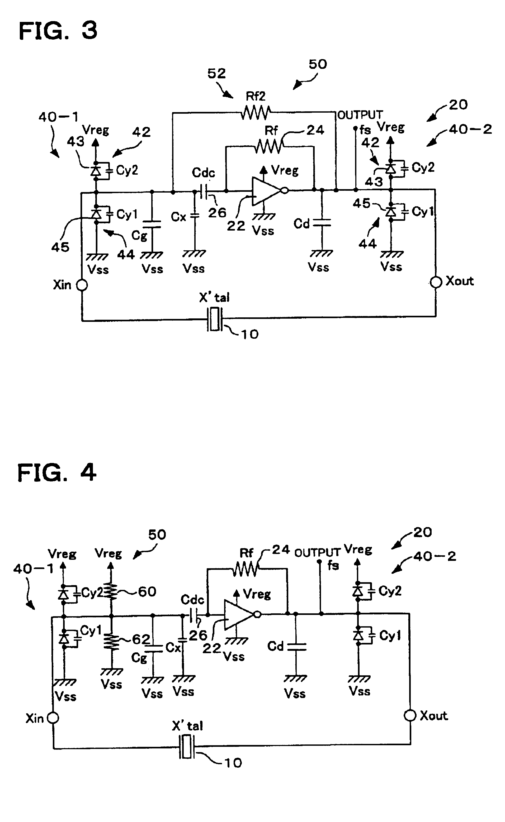
[0059]An oscillation circuit in accordance with a first embodiment is shown in FIG. 3.

[0060]This oscillation circuit comprises the crystal oscillator 10 that acts as an oscillation source, and the main circuit portion 20 that is connected by a signal path to this crystal oscillator 10 and is driven in oscillation.

[0061]The main circuit portion 20 is formed as a semiconductor device. More specifically, it is formed integrally on the semiconductor substrate and the two ends of the crystal oscillator 10 are connected to the input-output terminals Xin and Xout of the signal path thereof.

[0062]The main circuit portion 20 comprises the inverter 22 that is connected by the input-output terminals Xin and Xout to the crystal oscillator 10, the feedback resistor 24, and the DC-cutting capacitor 26 that acts as an element galvanically, or in a DC manner, separating the signal path provided between the input side of the inverter 22 and the input terminal Xin of the signal path.

[0063]However, if...

second embodiment

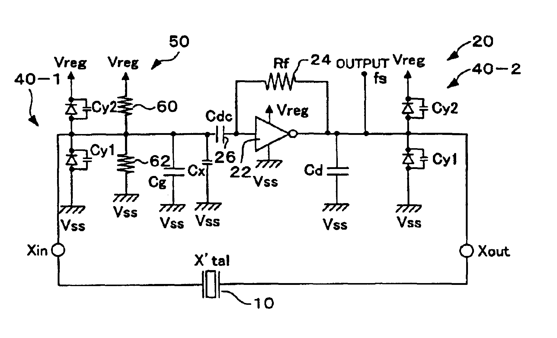
[0078]A second embodiment of the oscillation circuit in accordance with the present invention is shown in FIG. 4. Note that components that correspond to those of the embodiment shown in FIG. 3 are denoted by the same reference numbers and further description thereof is omitted.

[0079]In this embodiment, the potential stabilization circuit 50 uses a configuration that applies a bias voltage to the input terminal Xin side of the signal path through an element that functions as a resistor, to make the input terminal voltage stable.

[0080]In this case, bias resistors 60 and 62 are used as the previously described element that functions as a resistor. One bias resistor 60 is connected between the input terminal Xin side and the constant voltage Vreg side and the other bias resistor 62 is connected between the input terminal Xin side and the reference potential Vss side.

[0081]Use of the above-described configuration makes it possible to achieve operating effects similar to those of the fir...

third embodiment

[0089]A third embodiment of the oscillation circuit of the present invention is shown in FIG. 6. Note that components that correspond to those of the previous embodiments are denoted by the same reference numbers and further description thereof is omitted.

[0090]The characteristic of the potential stabilization circuit 50 of this embodiment is that it is configured so that the other end of the feedback resistor 24 that has one end connected to the output side of the inverter 22 is connected to the input terminal Xin of the signal path, instead of the input side of the inverter 22, stabilizing the potential of the input terminal Xin side.

[0091]Since the use of this configuration raises the danger of the potential of the input side of the inverter 22 becoming unstable, a configuration is used in which the input side of the inverter 22 is connected to the constant voltage Vreg and the reference potential Vss sides by the bias resistors 60 and 62.

[0092]Use of the above-described configur...


PUM


Abstract

This oscillation circuit includes a crystal oscillator and a main circuit portion connected by a signal path to the crystal oscillator and driven by the crystal oscillator. The main circuit portion is provided with a DC-cutting capacitor that galvanically separates the signal path between the input side of an inverter that is connected by the signal path to the crystal oscillator and an input terminal Xin of the signal path. A potential stabilization circuit is also provided, connecting the input terminal Xin of the signal path to the output side of the inverter through a resistance element.

Description

[0001]Japanese Patent Application No. 2002-201195, filed on Jul. 10, 2002, and Japanese Patent Application No. 2003-142196, filed on May 20, 2003, are hereby incorporated by reference in their entirety.BACKGROUND OF THE INVENTION[0002]The present invention relates to an oscillation circuit, an electronic apparatus, and a timepiece.[0003]The oscillation circuit used in a portable wristwatch or electronic apparatus often uses a battery or a rechargeable secondary battery as a main power source to drive electronic circuitry. The electronic circuitry that is used in such an appliance often creates a reference clock from the oscillation frequency fs of the oscillation circuit.[0004]An example of a conventional oscillation circuit is shown in FIG. 1.[0005]In this figure, a main circuit portion 20 of an oscillation circuit is formed on a semiconductor substrate, and this main circuit portion 20 is connected to the two ends of a crystal oscillator 10 by input-output terminals Xin and Xout t...

Claims


Application Information

Patent Timeline
Patent Type & Authority Patents(United States)
IPC IPC(8): H03B5/36H03B5/00H03B5/04G04G3/00H03B5/32
CPCH03B5/04H03B5/36
Inventor MIYAHARA, FUMIAKIKOIKE, KUNIOKAWAGUCHI, TAKASHINAKAMIYA, SHINJI
Owner SEIKO EPSON CORP
Why Eureka
Try Eureka