Polishing apparatus

a technology of polishing apparatus and polishing blade, which is applied in the direction of lapping machines, manufacturing tools, and abrasive surface conditioning devices, etc., can solve the problems of lowering the polishing rate, uneven polishing, and lowering the yield, and achieves the effect of reducing the necessary space of the apparatus and high accuracy

Inactive Publication Date: 2005-09-06
EBARA CORP
View PDF16 Cites 41 Cited by
  • Summary
  • Abstract
  • Description
  • Claims
  • Application Information

AI Technical Summary

Benefits of technology

[0012]The present invention has been made in view of the above drawbacks. It is therefore a first object of the present invention to provide a polishing apparatus comprising a dressing unit which can maintain good polishing performance of a polishing cloth used for polishing a semiconductor wafer, and thus can enhance the yield and productivity of polished semiconductor wafers, and to provide a dressing method for dressing the polishing cloth of the polishing apparatus.

Problems solved by technology

Therefore, if an identical polishing cloth 400 is repeatedly used for polishing semiconductor wafers W, problems such as lowered polishing rate and uneven polishing are caused.
If the clogged aggregation of the slurry (polishing liquid) or the polishing wastes are not removed from the polishing cloth, there is a high possibility that polishing particles and polishing wastes become attached to the polishing cloth to deteriorate a polishing function, or a surface, to be polished, of a semiconductor wafer is scratched, resulting in lowered yield.
This work is troublesome and disadvantageously lowers throughput of polished semiconductor wafers.
As a result, polishing cannot be performed during dressing, and hence a number of semiconductor wafers to be polished per unit time is decreased.
Thus, it is impossible to perform polishing in accordance with the above film thickness distribution, and hence a semiconductor substrate is excessively polished at portions having a small film thickness and is insufficiently polished at portions having a large film thickness.

Method used


Image

  • Polishing apparatus
  • Polishing apparatus
  • Polishing apparatus

Examples


first embodiment

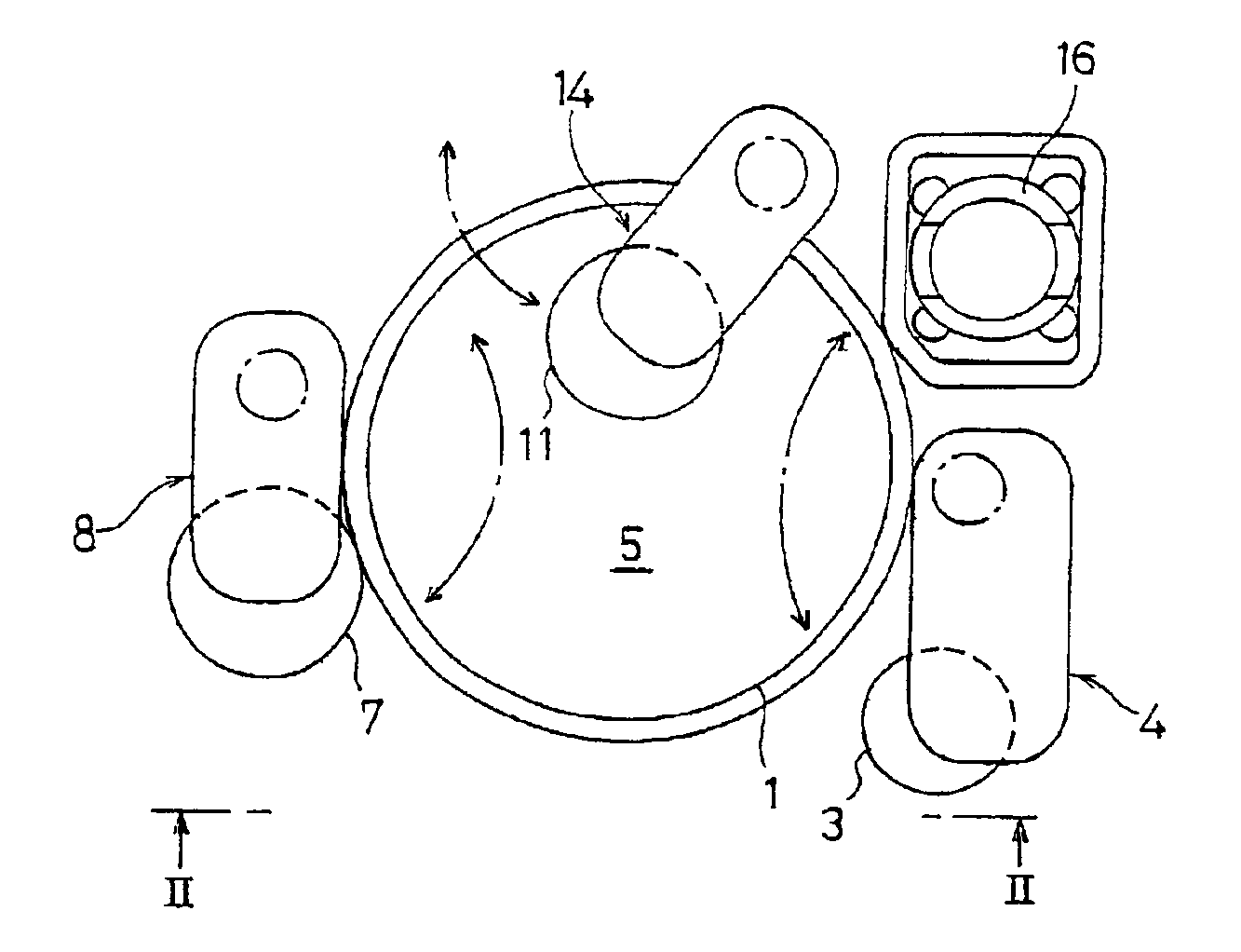
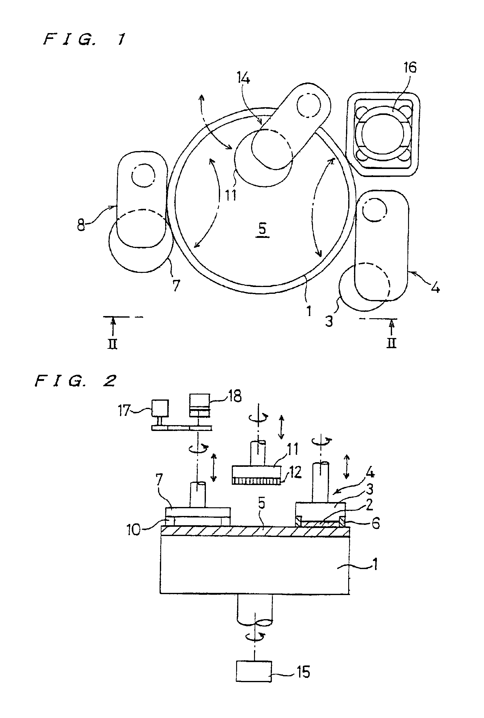
[0051]A polishing apparatus according to s the present invention will be described below with reference to FIGS. 1 through 5B. FIGS. 1 and 2 show an entire structure of the polishing apparatus according to the present invention, wherein FIG. 1 is a plan view, and FIG. 2 is a cross-sectional view taken along line II—II of FIG. 1. As shown in FIGS. 1 and 2, the polishing apparatus comprises a polishing table 1 and a top ring unit 4 having a top ring 3 for pressing a semiconductor wafer 2 against the polishing table 1 while holding the semiconductor wafer 2. The polishing table 1 is coupled to a motor 15 and is rotatable about a shaft of the motor 15, as indicated by an arrow. A polishing cloth 5 is attached to an upper surface of the polishing table 1.

[0052]The top ring unit 4 is horizontally swingable so that the top ring 3 can be positioned at a delivery position above a pusher 16 for delivering a semiconductor wafer 2, a polishing position on the polishing table 1, and a standby or...

second embodiment

[0066]Next, a polishing apparatus according to the present invention will be described below with reference to FIGS. 6 to 8.

[0067]FIGS. 6 and 7 are diagrams showing a polishing apparatus according to the second embodiment of the present invention, wherein FIG. 6 is a plan view, and FIG. 7 is a cross-sectional view taken along line VII—VII of FIG. 6. In FIGS. 6 and 7, the reference numeral 101 denotes a polishing table, reference numeral 103 denotes a top ring unit with a top ring 102, reference numeral 105 denotes a dressing unit with a dresser 104 having a diameter larger than that of a semiconductor wafer 111 as a workpiece to be polished, and the reference numeral 107 denotes a dressing unit with a dresser 106 having a diameter smaller than that of the semiconductor wafer 111 as the workpiece to be polished. The dresser 106 can be reciprocated along a guide rail 108. A pusher 109 for delivering a semiconductor wafer to the top ring 102 is provided adjacent to the polishing table ...

third embodiment

[0074]Next, a polishing apparatus according to the present invention will be described below with reference to FIGS. 10 through 17.

[0075]FIG. 10 is a schematic plan view showing the polishing apparatus according to the present embodiment.

[0076]As shown in FIG. 10, in the polishing apparatus according to the present embodiment, a pair of polishing sections 201a, 201b are disposed on one side of a space on a floor, which is rectangular as a whole, so as to laterally face each other. A pair of load / unload units for placing thereon cassettes 202a, 202b for accommodating semiconductor wafers are disposed on another side of the space. Two transfer robots 204a, 204b for transferring a semiconductor wafer are disposed on a line connecting the polishing sections 201a, 201b to the load / unload units to constitute a transfer line. One inverter 205 or 206 is disposed on each side of the transfer line, respectively, and two cleaning units 207a and 208a, or 207b and 208b are disposed with the inve...


PUM

PropertyMeasurementUnit
widthaaaaaaaaaa
diameteraaaaaaaaaa
lengthaaaaaaaaaa

Abstract

The present invention relates to a polishing apparatus for polishing a workpiece, such as a semiconductor wafer, to a flat mirror finish. The polishing apparatus comprises a polishing table having a polishing surface, and a top ring, and the workpiece is interposed between the polishing table and the top ring, and pressed at a predetermined pressure to polish the workpiece. The polishing apparatus comprises at least two dressing units for dressing the polishing surface by being brought into contact with the ppolishing surface, which is a surface of a polishing cloth.

Description

TECHNICAL FIELD[0001]The present invention relates to a polishing apparatus for polishing a workpiece, such as a semiconductor wafer, to a flat mirror finish, and more particularly to a polishing apparatus comprising a dresser for dressing a surface of a polishing cloth attached to an upper surface of a polishing table.BACKGROUND ART[0002]As semiconductor devices have become more highly integrated in recent years, circuit interconnections have become finer and a distance between these circuit interconnections have become smaller. In case of photolithography which can form interconnections that are at most 0.5 μm wide, it is required that surfaces on which pattern images are to be focused by a stepper should be as flat as possible because a depth of focus of an optical system is relatively small. A polishing apparatus for performing chemical mechanical polishing (CMP) has been used for planarizing a semiconductor wafer.[0003]In a polishing apparatus for polishing and planarizing a su...

Claims


Application Information

Patent Timeline
Patent Type & Authority Patents(United States)
IPC IPC(8): B24B53/00B24B37/04B24B53/007B24B53/017H01L21/306
CPCB24B29/005B24B53/003B24B53/017H01L21/30625H01L21/304
Inventor KAMIMURA, KENJIKIMURA, NORIOOKAMURA, SATOSHIAIZAWA, HIDEOAKAGI, MAKOTOTOKUSHIGE, KATSUHIKOMATSUO, HISANORITSUJIMURA, MANABU
Owner EBARA CORP
Why Eureka
Try Eureka