Wire saw and process for slicing multiple semiconductor ingots

a technology of wire saw and semiconductor ingot, which is applied in the direction of metal sawing device, manufacturing tools, working accessories, etc., can solve the problems of requiring a substantial amount of time, affecting the efficiency of wafer production, and difficulty in implementing a more rapid wire sawing process, so as to improve the throughput of slicing semiconductor ingot and high quality

Inactive Publication Date: 2005-09-13
GLOBALWAFERS CO LTD
View PDF19 Cites 53 Cited by
  • Summary
  • Abstract
  • Description
  • Claims
  • Application Information

AI Technical Summary

Benefits of technology

[0008]Among the several objects and features of the present invention may be noted the provision of an apparatus and process to improve throughput in slicing semiconductor ingots into wafers; the provision of such an apparatus and process that simultaneously slice multip

Problems solved by technology

A limitation to the process of slicing semiconductor ingots is that it requires a substantial amount of time and can become a hindrance to the efficient production of wafers.
It is desirable to slice the ingots as quickly as possible to improve throughput and red

Method used


Image

  • Wire saw and process for slicing multiple semiconductor ingots
  • Wire saw and process for slicing multiple semiconductor ingots
  • Wire saw and process for slicing multiple semiconductor ingots

Examples


Embodiment Construction

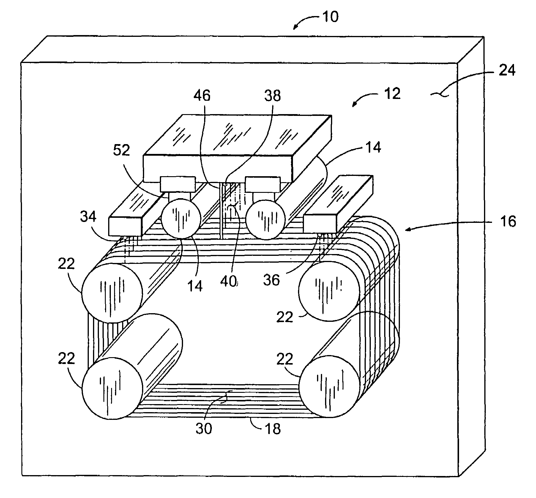
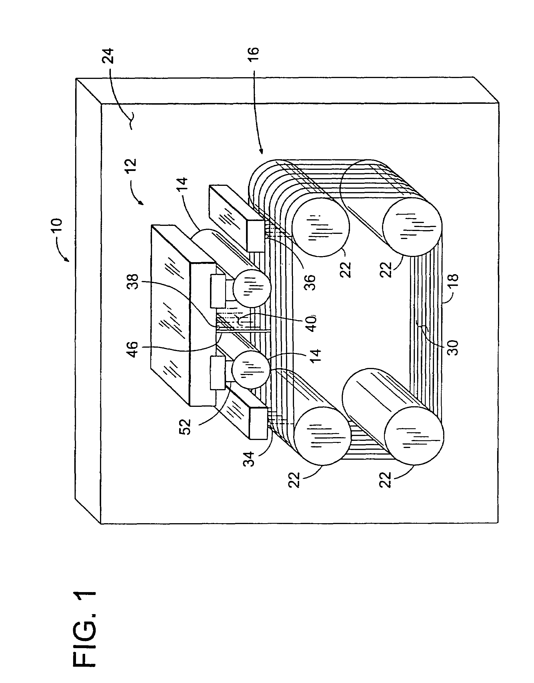
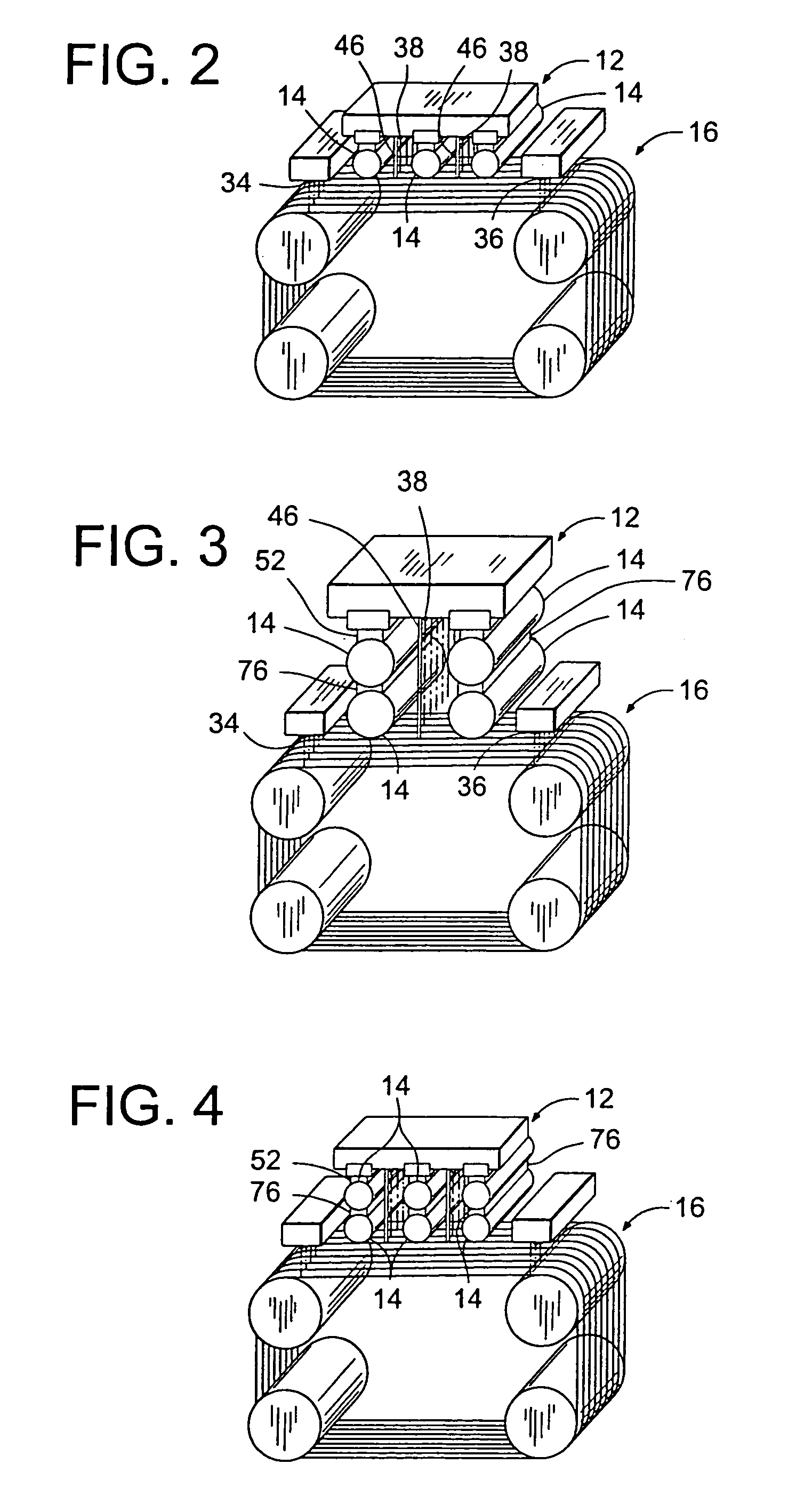
[0027]Referring now to the drawings and in particular to FIG. 1, a wire saw of the present invention for simultaneously slicing a plurality of semiconductor ingots into wafers is indicated generally at 10. The wire saw 10 has an ingot support generally indicated at 12 for holding ingots 14. A cutting head indicated generally at 16 mounts a wire 18 for reciprocal movement to cut ingots. The ingot support 12 is configured for holding conventional monocrystalline silicon ingots 14, which are generally cylindrical in shape, in a generally side-by-side arrangement with longitudinal axes of the ingots being non-collinear and approximately parallel. Ingots 14 are sliced when they are engaged against the moving cutting wire 18 in the presence of an abrasive liquid slurry. The ingot support 12 and cutting head 16 are moveable relative to each other so that the ingots 14 may be moved into or out of engagement with the cutting wire 18, and other relative movements between the cutting head and ...


PUM

PropertyMeasurementUnit
Temperatureaaaaaaaaaa
Pressureaaaaaaaaaa
Lengthaaaaaaaaaa

Abstract

A wire saw (10) for simultaneously slicing multiple, generally cylindrical monocrystalline ingots (14) into wafers. The wire saw includes a cutting head (16), an ingot support (12), and multiple generally parallel lengths of cutting wire (18) defining a cutting web (30). A slurry delivery system includes nozzles (34, 36, and 38) positioned for dispensing slurry along the wire web generally at lateral sides of each ingot. A process for simultaneously slicing at least two generally cylindrical semiconductor ingots into wafers includes mounting at least two ingots to a common ingot support, moving the ingot support relative to the cutting web so that the two ingots simultaneously press against the cutting web at cutting regions, and dispensing a liquid slurry to at least three locations on the wire web including two outermost sides of the cutting regions and a location between each pair of ingots.

Description

BACKGROUND OF THE INVENTION[0001]This invention relates generally to cutting monocrystalline semiconductor ingots into multiple wafers, and in particular to an apparatus and method for simultaneously slicing at least two semiconductor ingots to improve throughput.[0002]Semiconductor wafers are generally prepared from a single crystal ingot, such as a silicon ingot, that is cylindrical in shape. The ingot is sliced in a direction normal to its longitudinal axis to produce as many as several hundred thin, disk-shaped wafers. The slicing operation may be accomplished by means of a wire saw, wherein the ingot is contacted with a reciprocating wire while a liquid slurry containing abrasive grains is supplied to a contact area between the ingot and the wire. As the abrasive particles in the slurry are rubbed by the wire against the ingot, silicon crystal is removed and the ingot is gradually sliced. The wire saw provides a gentle mechanical method for slicing which makes it ideal for cutt...

Claims


Application Information

Patent Timeline
IPC IPC(8): B23D57/00B28D5/00B28D1/02B24B27/06B28D5/04H01L21/304
CPCB23D57/0061B28D1/025B28D5/0082
Inventor ZAVATTARI, CARLOSEVERICO, FERDINANDODE MARIA, PAOLO
Owner GLOBALWAFERS CO LTD
Why Eureka
Try Eureka