Method of manufacturing the semiconductor device

a manufacturing method and semiconductor technology, applied in the direction of semiconductor devices, capacitors, electrical devices, etc., can solve the problems of natural decrease of electric charge usable as remanent polarization, degradation of property, fatigue phenomenon, etc., and achieve the improvement of crystallinity, excellent crystalline quality, and the effect of increasing the reliability of the semiconductor devi

Inactive Publication Date: 2005-09-13
FUJITSU LTD
View PDF7 Cites 15 Cited by
  • Summary
  • Abstract
  • Description
  • Claims
  • Application Information

AI Technical Summary

Benefits of technology

[0011]Accordingly, it is a general object of the present invention to provide a capacitor in which the above-described disadvantage is eliminated.
[0017]According to the above-described semiconductor devices, the electrodes are provided perpendicular to the direction of the polarization axis of the ferroelectric film in the capacitor. Accordingly, the maximum remanent polarization of the ferroelectric film can be extracted. Therefore, the above-described semiconductor devices have tolerance to the degradation of a remanent polarization charge and have a high signal-to-noise ratio at the time of reading out information. Accordingly, the reliability of the semiconductor devices can be increased.
[0019]According to the above-described method, since the ferroelectric film of the capacitor is formed on the single-crystal substrate, the ferroelectric film may be formed epitaxially thereon. Therefore, the ferroelectric film can be formed with excellent crystalline quality with a fixed crystal orientation. Further, in the semiconductor device, the capacitor is formed in a process independent of the process of forming the transistor. Accordingly, a wide range of tolerance can be set for the conditions for forming the capacitor, such as a temperature condition, so that the ferroelectric film may be formed with better crystallinity. As a result, the reliability of the semiconductor device can be increased.

Problems solved by technology

Generally, in PZT, remanent polarization is reduced as the reversal of polarization is repeated, causing property degradation (fatigue phenomenon).
This results in the problem that an electric charge usable as remanent polarization decreases naturally.

Method used


Image

  • Method of manufacturing the semiconductor device
  • Method of manufacturing the semiconductor device
  • Method of manufacturing the semiconductor device

Examples


Embodiment Construction

[0030]First, a brief description is given of the principles of the present invention.

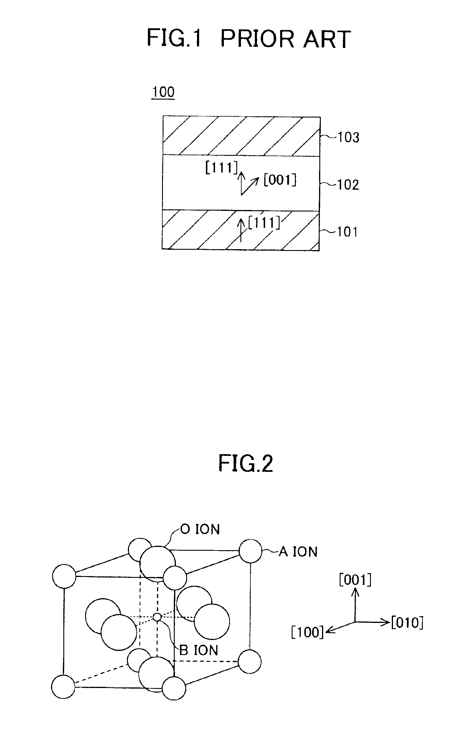
[0031]In the following, the case of using a perovskite oxide (an oxide having a perovskite structure) as the ferroelectric film of a ferroelectric capacitor is described as an example. Generally, a perovskite oxide is expressed by the general formula ABO3. FIG. 2 is a diagram showing a perovskite structure. Referring to FIG. 2, in an ideal perovskite structure, a unit lattice is a cube with A ions being disposed at the vertexes, a B ion at the body center, and C ions at the face centers. In this structure, the large-size A and O ions form a cubic closest packing structure with the small-size B ion being in the space formed therein. If the oxide is PZT, the A ions are Pb2+ and the B ions are Zr4+ and Ti4+. The spontaneous polarization of a ferroelectric is caused by asymmetrical displacement of the B ions, which are small and mobile, and is reversible by an external electric field. The B ions are mos...


PUM


Abstract

A method of manufacturing semiconductor device including a capacitor including a pair of electrodes and a ferroelectric flu with ferroelectricity sandwiched therebetween, by depositing the ferroelectric film on first substrate; forming the capacitor by grinding the ferroelectric film and forming the electrodes so that the electrodes are perpendicular to a direction of a polarization axis of the ferroelectric film; forming a first interlayer insulating film covering a surface of the first substrate and the capacitor; forming a transistor on a second substrate, the transistor including a ate electrode and a diffusion region; forming a second interlayer insulating film covering a surface of the second substrate and the transistor; flattening surfaces of the first and second interlayer insulating films by chemical mechanical polishing; integrating the first and second substrates by joining the flattened surfaces of the first and second interlayer insulating films; and removing the first substrate.

Description

CROSS-REFERENCE TO RELATED APPLICATION[0001]The present application is based on Japanese Laid-Open Patent Application No. 2002-358093, filed on Dec. 10, 2002, the entire contents of which are hereby incorporated by reference.BACKGROUND OF THE INVENTION[0002]1. Field of the Invention[0003]The present invention generally relates to a capacitor, a semiconductor device including the capacitor, and a method of manufacturing the semiconductor device, and more particularly to a nonvolatile semiconductor storage device including a capacitor using a ferroelectric material as a dielectric.[0004]2. Description of the Related Art[0005]Some semiconductor devices, particularly, semiconductor memories, have a variety of properties. The semiconductor memories are roughly classified into volatile memories that lose information stored therein when power is turned off and nonvolatile memories that retain information stored therein when power is turned off. A nonvolatile memory that retains data in a c...

Claims


Application Information

Patent Timeline
Patent Type & Authority Patents(United States)
IPC IPC(8): H01L21/02H01L21/70H01L21/768H01L27/105H01L21/8246H01L27/115H01L27/11507
CPCH01L27/11502H01L27/11507H01L28/55H01L28/90H01L21/76838H10B53/30H10B53/00
Inventor MARUYAMA, KENJI
Owner FUJITSU LTD
Why Eureka
Try Eureka