Multi beam charged particle device

Inactive Publication Date: 2005-09-13
ICT INTEGRATED CIRCUIT TESTING GESELLSCHAFT FUER HALBLEITERPRUEFTECHNIK GMBH
View PDF23 Cites 117 Cited by
  • Summary
  • Abstract
  • Description
  • Claims
  • Application Information

AI Technical Summary

Benefits of technology

[0012]The present invention provides an improved column for a charged particle beam device. The column comprises an aperture plate having multiple apertures to produce multiple beams of charged particles and a deflector to influence the beams of charged particles so that each beam appears to come from a different source. Furthermore, an objective lens is used in order to focus the charged-particle beams onto the specimen. Due to the deflector, multiple images of the source are created on the surface of the specimen whereby all the images can be used for parallel data acquisition and/or for parallel modification of the specimen. Accordingly, the speed of data acquisition (modification) is increased. With regard to the focusing properties of the objective lens, the beams of charged particles can basically be treated as independent particle beams which do not negatively affect each other. Accordingly, each beam basically provides the same resolution as the beam a conventional charged particle beam device.
[0013]According

Problems solved by technology

However, the inspection of wafers or masks for defects requires the examination of the whole wafer or mask area.
However, because only one very narrow electron beam is used for scanning, a long time is required to scan the entire surface of the wafer.
Accordingly, it is not feasible to use a conventional (single-beam) Scanning Electron Microscope (SEM) for wafer inspection, since this approach does not provide the required throughput.
However, both approaches have not yet been put into industrial practice.
However, the apparatus according to U.S. Pat. No. 5,892,224 is primarily designed for the inspection of ma

Method used


Image

  • Multi beam charged particle device
  • Multi beam charged particle device
  • Multi beam charged particle device

Examples


second embodiment

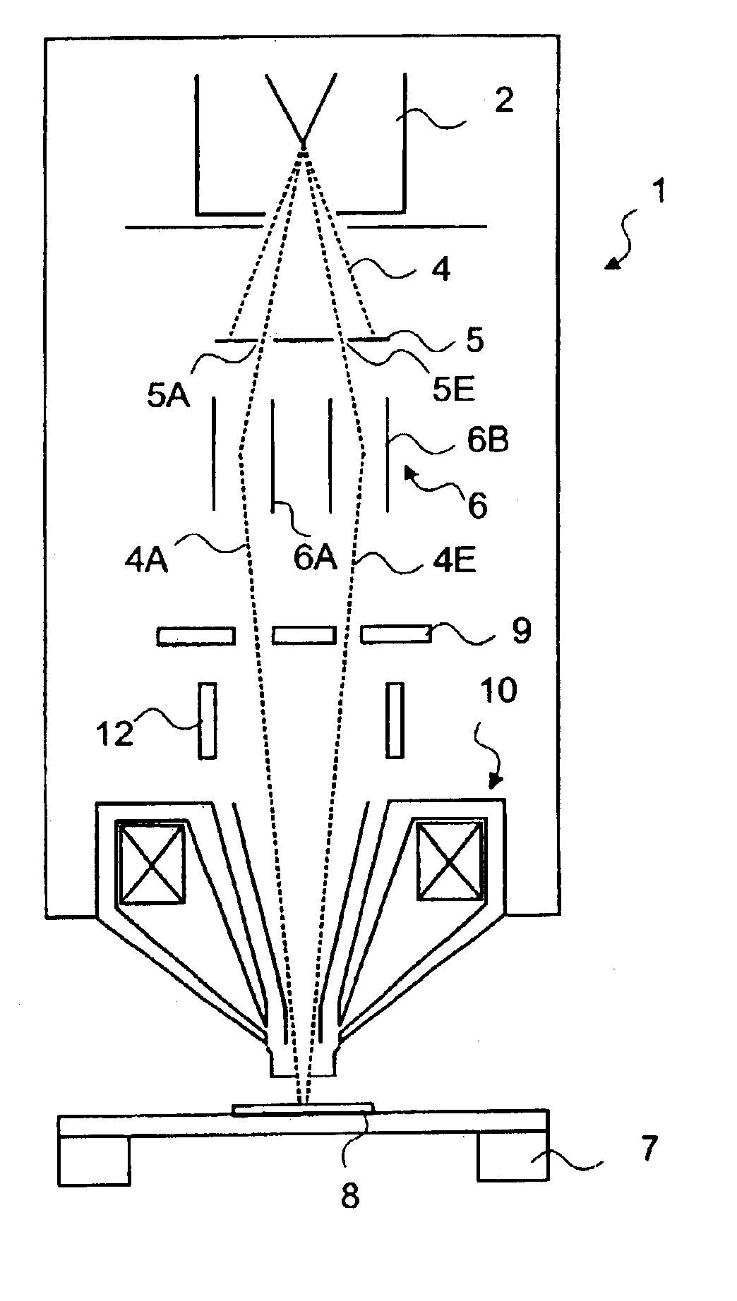
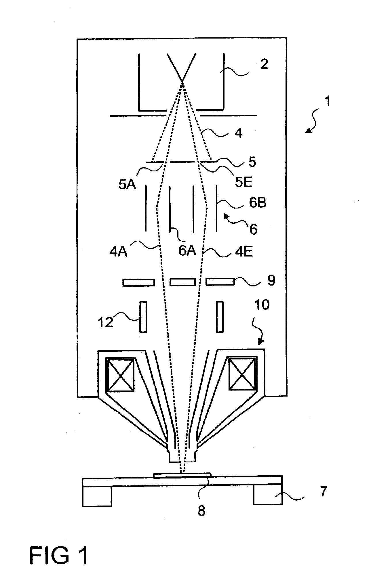
[0046]FIG. 7 shows schematically a column according to the present invention. This embodiment is similar to that of FIG. 1, except for the following; The column comprises a beam selector 16 located right after the particle source 2. The beam selector 16 comprises a first deflector 16A, aperture plate 16B, a second deflector 16C, and a third deflector 16D. The aperture plate 16B comprises two apertures having two different diameters. After the beam of charged particles leaves the particle source 2, the first deflector 16A deflects the charged particle beam 4 towards one the two aperture in the aperture plate I&B. Thereafter, the second and the third deflector bring the charged particle beam 4 back to its way along the optical axis of the column.

[0047]The aperture plate 15 used in FIG. 7 comprises, in addition to the apertures 15A-15H situated along a ring parallel to the edge of the aperture plate, a further aperture 151 situated in the center of the aperture plate (see FIG. 8). Acco...

third embodiment

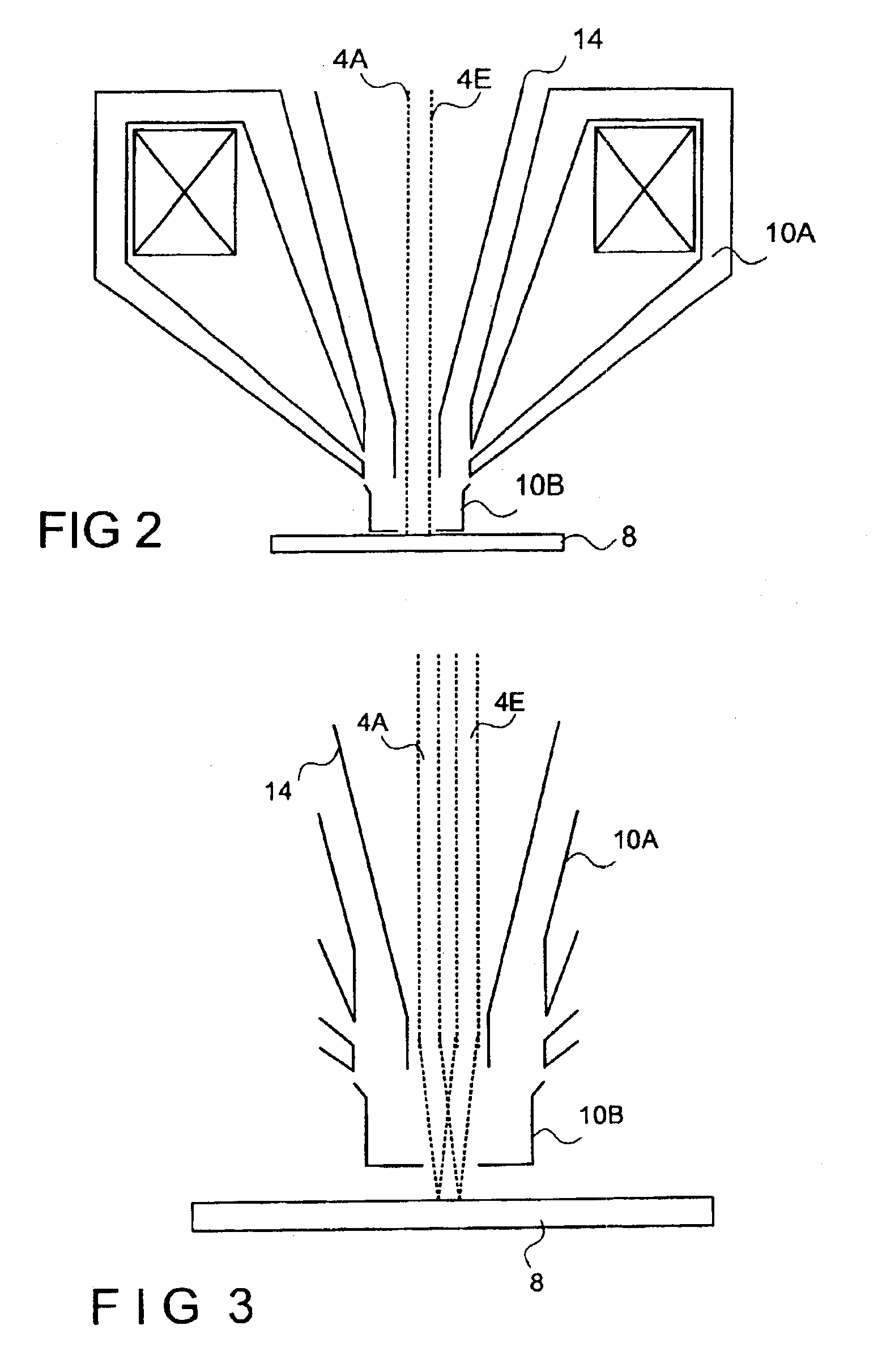
[0051]FIG. 10 shows schematically a column according to the present invention. This embodiment is also similar to that of FIG. 1, except for the following; After leaving the charged particle source 2, the charged particle beam 4 passes through the aperture plate 25 having four apertures 25A-25D which are situated at equal distance along a ring on the aperture plate 25. By passing through the aperture plate 25, four charged particle beams 4A-4D are created. Thereafter, the deflectors 26A-26D are used to influence the beams of charged particles 4A-4D so that each beam 4A-4D appears to come from a different source. The deflectors 26A-26D influence each of the beams 4A-4D individually which leads to a better control of the properties of each individual beam.

[0052]The charged particle beams 4A-4D then pass the detector 29 which is used to detect those particles that come from the specimen 8 in order to produce multiple images of the specimen 8. The detector 29 is divided in multiple segm...


PUM


Abstract

The present invention provides an improved column for a charged particle beam device. The column comprises an aperture plate having multiple apertures to produce multiple beams of charged particles and a deflector to influence the beams of charged particles so that each beam appears to come from a different source. Furthermore, an objective lens is used in order to focus the charged-particle beams onto the specimen. Due to the deflector, multiple images of the source are created on the surface of the specimen whereby all the images can be used for parallel data acquisition. Accordingly, the speed of data acquisition is increased. With regard to the focusing properties of the objective lens, the beams of charged particles can basically be treated as independent particle beams which do not negatively affect each other. Accordingly, each beam basically provides the same resolution as the beam of a conventional charged particle beam device.

Description

[0001]This is a National stage entry under 35 U.S.C. § 371 of Application No. PCT / EP01 / 04787 filed Apr. 27, 2001; the disclosure of which is incorporated herein by reference.FIELD OF THE INVENTION[0002]The invention relates to an apparatus for the examination of specimen with charged particles. In particular, this invention relates to an apparatus for the examination of specimen with multiple beams of charged particles.BACKGROUND OF THE INVENTION[0003]Modern semiconductor technology is highly dependent on an accurate control of the various processes used during the production of integrated circuits. Accordingly, the wafers have to be inspected repeatedly in order to localize problems as early as possible. Furthermore, a mask or reticle should also be inspected before its actual use during wafer processing in order to make sure that the mask accurately defines the desired pattern. This is done because any defects in the mask pattern will be transferred to the substrate (e.g., wafer) ...

Claims


Application Information

Patent Timeline
IPC IPC(8): H01J37/09H01J37/04H01J37/26G01Q30/02
CPCH01J37/04H01J37/09H01J37/266
Inventor ADAMEC, PAVELDEGENHARDT, RALFFEUERBAUM, HANS-PETERMUNACK, HARRYWINKLER, DIETER
Owner ICT INTEGRATED CIRCUIT TESTING GESELLSCHAFT FUER HALBLEITERPRUEFTECHNIK GMBH
Why Eureka
Try Eureka