Semiconductor integrated circuit

a technology of integrated circuits and semiconductors, applied in the direction of semiconductor devices, semiconductor/solid-state device details, diodes, etc., can solve the problems of large potential difference between gate gates, esd (electro-static discharge) becomes an important issue, and semiconductor integrated devices often become defective products. , to achieve the effect of improving the ability to stand voltag

Inactive Publication Date: 2005-09-13
LONGITUDE SEMICON S A R L
View PDF17 Cites 15 Cited by
  • Summary
  • Abstract
  • Description
  • Claims
  • Application Information

AI Technical Summary

Benefits of technology

[0021]It is therefore an objective of the present invention to provide an semiconductor integrated circuit which has an improved withstanding voltage for the electrostatic breakdown according to the charged device model by connecting a MOS capacitor between the power source wire and the ground potential wire as the element to be protected.

Problems solved by technology

As the semiconductor integrated circuits becomes finer, and the level of integration advances, a phenomenon called ESD (electro-static discharge) becomes an important issue, because electrostatic breakdown is caused by the electro-static charge.
As automatic manufacturing processes advance, semiconductor integrated devices often become defective products because of electrification of the devices according to the charged device model by friction or contact with manufacturing equipment during automated test processes and automated assembly processes for electronic machines.
As a result, a large potential difference is generated between the gate and the source of the MOS transistor of the internal circuit, and dielectric breakdown occurs.

Method used


Image

  • Semiconductor integrated circuit
  • Semiconductor integrated circuit
  • Semiconductor integrated circuit

Examples


first embodiment

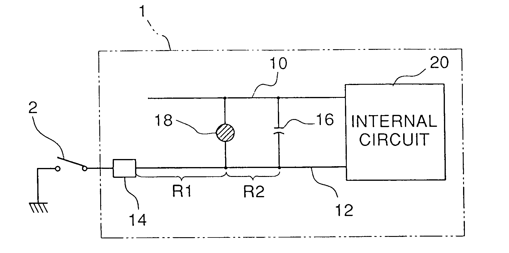
[0065]When the discharge test switch 2 is turned on after the semiconductor integrated circuit device is subjected to electrification, the charge charged in the capacitance held by the ground potential wire 12 from the ground terminal 14 is discharged to the ground. At this time, the voltage between both terminals of the MOS capacitor is clamped at a voltage lower than the dielectric breakdown voltage by the electrostatic protection element 18. Thus, the MOS capacitor is protected from the electrostatic breakdown.

[0066]Here, the wire resistance of the ground potential wire 12 must be taken into consideration in order to protect the MOS capacitor. That is, in order to protect the MOS capacitor from electrostatic breakdown by the charged device model, it is necessary to satisfy the following equation (1),

VC+R2·

wherein VC is the clamp voltage of the electrostatic protection element 18, i is a current flowing in the wire resistance R2 of the ground potential wire 12 at the time of ...

third embodiment

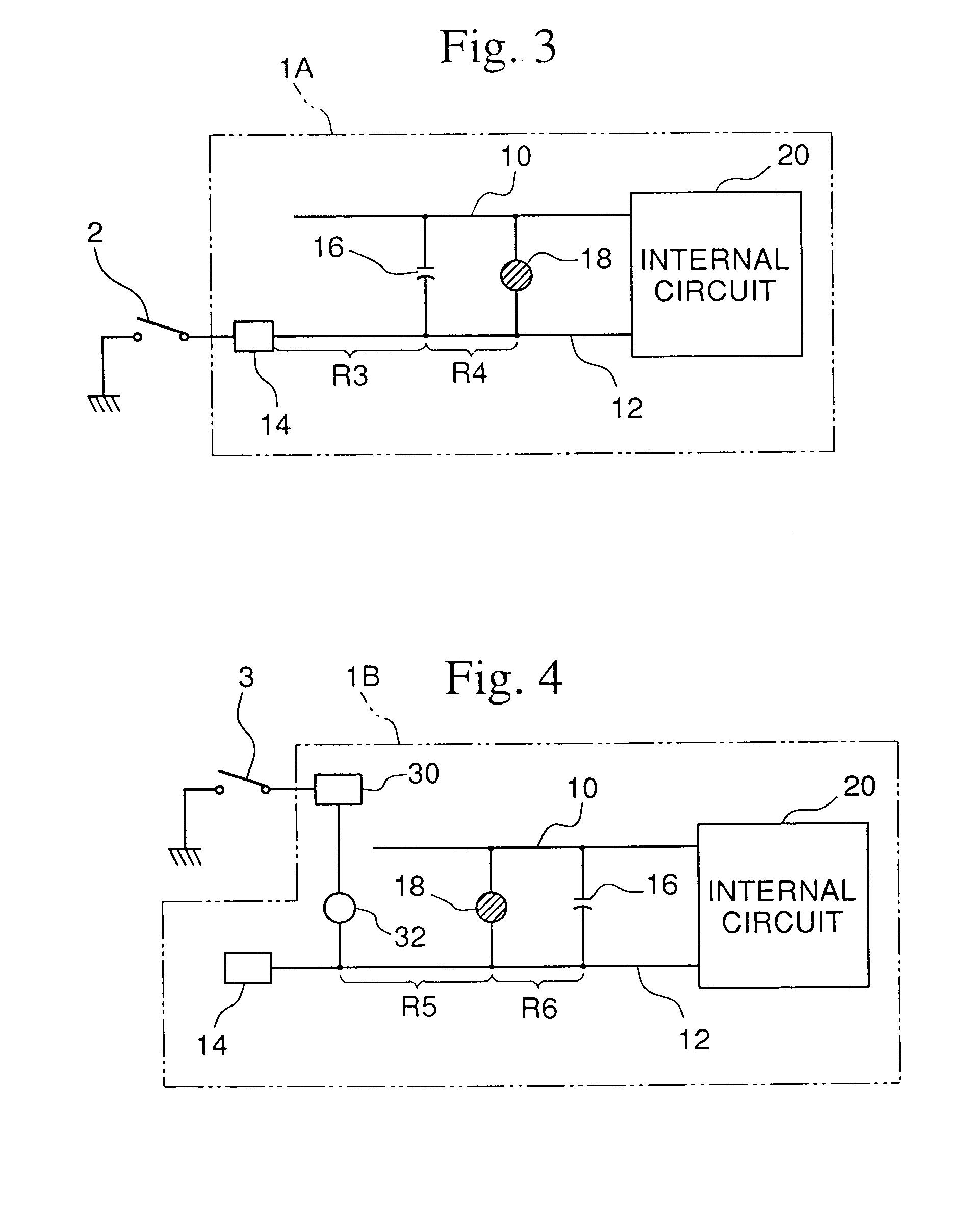
[0078]Next, a semiconductor integrated circuit device according to the present invention is illustrated in FIG. 4. As shown in FIG. 4, the semiconductor integrated circuit device 1B comprises an input / output terminal 30, an electrostatic protection element 32, one end of which is connected to the input / output terminal 30 and the other end of which is connected to the ground potential wire 12, and a MOS capacitor 16, one end of which is connected to the power source wire and the other end of which is connected to the ground potential wire 12. The input / output terminal 30 is connected to ground through the discharge test switch 3 for preparing the CDM test. Here, the input / output terminal 30 means an input terminal, an output terminal, or a terminal for use both as input and output (I / O).

[0079]The electrostatic protection element (CDM protection circuit) 30 is connected in parallel with the MOS capacitor between the ground terminal and the MOS capacitor 16. This electrostatic protecti...

fifth embodiment

[0099]The structure of a semiconductor integrated circuit element 1D according to the present invention is shown in FIG. 6. As shown in FIG. 6, the semiconductor integrated circuit device 1D comprises an input / output terminal 30 and a ground terminal 14. The semiconductor integrated circuit device 1D further comprises a first ground potential wire 34 for supplying a ground potential and a second ground potential wire 35, connected commonly with the first ground potential wire to the ground terminal 14 for supplying the ground potential.

[0100]The semiconductor integrated circuit device 1d comprises the electrostatic protection element 32, one end of which is connected to the input / output terminal 30, and the other end of which is connected to the first ground potential wire 34, and the MOS capacitor, one end of which is connected to the power source wire 10 and the other end of which is connected to the second ground potential wire 35. A diffusion layer 136 is connected to the second...


PUM


Abstract

A semiconductor integrated circuit is provided, which has an improved withstanding voltage for electrostatic breakdown at the time of electrostatic discharge by the charged device model, in the case of protecting a MOS capacitor provided at the input side of the internal circuit. The semiconductor integrated circuit comprises an internal circuit 20 for inputting an external signal, an internal circuit MOS capacitor 16, one end of which is connected to a power source wire 10 for supplying the source voltage and the other end of which is connected to a ground potential wire 12 for supplying the ground potential; a ground terminal 14 to which one end of the ground potential wire is connected; an electrostatic protection element 18 connected in parallel with the MOS capacitor 16 between the ground terminal 14 and the MOS capacitor, wherein the MOS capacitor and the electrostatic protection element are connected between the power source wire and the ground potential wire such that the wire resistance R1 of the ground potential wire between the ground terminal and the connection point with one end of the electrostatic protection element is larger than the wire resistance R2 of the ground potential wire between the connection point with one end of the electrostatic protection element and the connection point with one end of the MOS capacitor.

Description

BACKGROUND OF THE INVENTION[0001]1. Field of the Invention[0002]The present invention relates to a semiconductor integrated circuit, and in particular, relates to a semiconductor integrated circuit capable of preventing electrostatic breakdown caused by the electrostatic discharge by the charged device model.[0003]2. Background Art[0004]As the semiconductor integrated circuits becomes finer, and the level of integration advances, a phenomenon called ESD (electro-static discharge) becomes an important issue, because electrostatic breakdown is caused by the electro-static charge. As is well known, three models including a human-body model (HBM), a machine model (MM), and a charged device model (CDM) have been proposed for explaining the generation of the electro-static charge breakdown. The human body model is a model in which the breakdown of the device is caused by the discharge of an electrostatic charge accumulated in a human body to the device when the human body touches the devi...

Claims


Application Information

Patent Timeline
Patent Type & Authority Patents(United States)
IPC IPC(8): H01L29/66H01L21/70H01L23/58H01L29/78H01L23/62H01L21/822H01L21/8234H01L27/085H01L27/088H01L27/04
CPCH01L27/0251H01L27/0629H01L27/0647H01L27/0676H01L27/0811H01L2924/0002H01L2924/00H01L27/04
Inventor HORIGUCHI, YOKO
Owner LONGITUDE SEMICON S A R L
Why Eureka
Try Eureka