Micro electro mechanical system controlled organic LED and pixel arrays and method of using and of manufacturing same

a micro electro mechanical and organic technology, applied in microstructural technology, microstructural devices, discharge tubes/lamp details, etc., can solve the problems of large digital assistants (pdas), portable nature, and display cannot withstand large amounts of mechanical vibration and/or pressur

Inactive Publication Date: 2005-09-13
GENERAL ELECTRIC CO
View PDF16 Cites 50 Cited by
  • Summary
  • Abstract
  • Description
  • Claims
  • Application Information

AI Technical Summary

Benefits of technology

[0009]Organic light emitting devices use a micro electromechanical system (MEMS) structure to control the display characteristics of a pixel and/or a pixel array wherein each pixel contains a MEMS and an OLED element. A MEMS structure is used for controlling the OLED element, for example, switching the OLED element on and off, and controlling the intensity of the OLED. The MEMS controlled OLED pixels can be fabricated on a flexible subs...

Problems solved by technology

Due to the brittle nature of glass, the displays cannot withstand large amounts of mechanical vibration and/or pressure.
This can be a major disadvantage for portable display applications, such as portable digital assistants (PDAs), which by their portable nature, can be exposed to a large amount of shock and abuse.
Also, the properties of the LCD limit the operating temperature range of the device.
These requirements preclude the use of a flexible substrate, such as a polymer substrate, for the FED because flexure of the substrate would cause the spacing size to move out of...

Method used


Image

  • Micro electro mechanical system controlled organic LED and pixel arrays and method of using and of manufacturing same
  • Micro electro mechanical system controlled organic LED and pixel arrays and method of using and of manufacturing same
  • Micro electro mechanical system controlled organic LED and pixel arrays and method of using and of manufacturing same

Examples


first embodiment

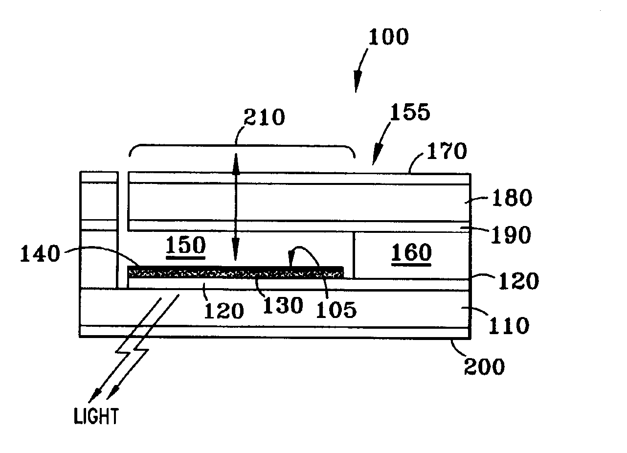
[0018]the invention is shown in FIG. 1. A light emitting element 100 comprises an OLED and a MEMS. The OLED 105 includes an anode 120, an organic light emitting layer 130, and a cathode 140. The OLED 105 may be formed on a transparent substrate 110, for example. The transparent substrate 110 can be a glass, polymer or other transparent material. If the substrate comprises a polymer, a sealant layer 200 can be provided to protect the OLED from air and moisture absorption through the substrate 110.

[0019]The organic light emitting layer 130 emits light upon application of a voltage across the anode and cathode. The anode and cathode inject charge carriers, i.e. holes and electrons, into the organic light emitting layer 130 where they recombine to form excited molecules or excitons which emit light when the molecules or excitons decay. The color of light emitted by the molecules depends on the energy difference between the excited state and the ground state of the molecules or excitons....

second embodiment

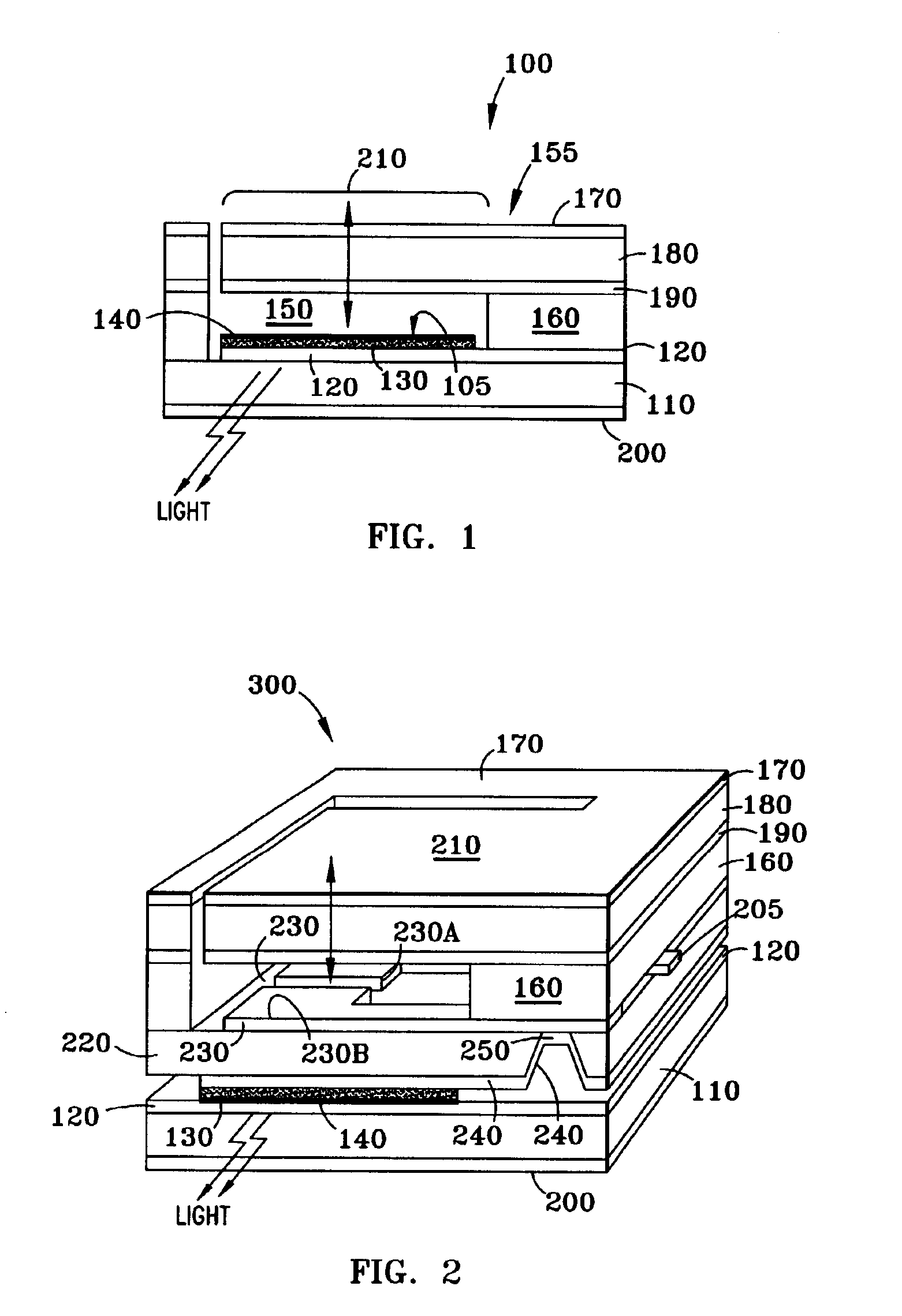
[0031]the invention is illustrated in FIG. 2. The light emitting element 300 comprises a transparent substrate 110, an anode 120, an organic light emitting layer 130, a cathode 140, a cavity 150, a spacer 160, a first conductive layer 170, an actuating member 180, a second conductive layer 190, and an optional sealant layer 200.

[0032]The light emitting element 300 also comprises a MEMS substrate 220, e.g. of polyimide, on which is patterned a contact layer 230 comprising contacts 230A and 230B. Contact 230A, which extends to 205, is connected to one side of the control voltage applied across the OLED. Contact 230B is electrically connected to the cathode 140 of the OLED by means of a connecting member 240. Thus, when the MEMS is activated, the cantilever 210 is forced downward, and the conductive layer 190 touches both contacts 230A and 230B to apply the control voltage across the OLED. The current flows from 205 to 230A to 190 to 230B to 240 to the cathode 140 of the OLED and acros...


PUM


Abstract

Organic light emitting devices are disclosed that use a micro electromechanical system (MEMS) structure to enable a pixel and pixel array wherein each pixel contains a MEMS and an OLED element. A MEMS structure is used for switching the OLED element. These OLED/MEMS pixels can be fabricated on flex circuit, silicon, as well as other inorganic materials. They can be fabricated in a large array for developing a 2-dimensional display application and each pixel can be addressed through conventional matrix scanning addressing scheme. The ability of fabricating these OLED/MEMS pixels on flexible organic substrates as well as other rigid substrates enables wider selection of substrate materials for use with different applications.

Description

CROSS REFERENCE TO RELATED APPLICATION[0001]This patent application is a continuation application of U.S. patent application having Ser. No. 09 / 618,665, now U.S. Pat. No. 6,677,709 filed on Jul. 18, 2000, which is incorporated herein by reference in its entirety. Applicants claim the benefit of the filing date of U.S. patent application Ser. No. 09 / 618,665.BACKGROUND OF THE INVENTION[0002]The present invention relates generally to light emitting elements and displays. More particularly, the present invention relates to an organic light emitting device that is controlled by a micro electromechanical system, a display constructed thereof, and a method of using and manufacturing the same.[0003]Current flat panel liquid crystal display (LCD) technology uses a rigid substrate, such as glass, with thin film transistors (TFTs) corresponding to each display pixel. Due to the brittle nature of glass, the displays cannot withstand large amounts of mechanical vibration and / or pressure. This ca...

Claims


Application Information

Patent Timeline
IPC IPC(8): B81B7/00B81B7/02G09G3/32H01L27/32H01L51/52H01L27/28H01L51/50B81B3/00G09F9/30G09G3/20G09G3/30H05B33/06H05B33/10H05B44/00
CPCG09G3/3216G09G3/346H01L27/3225G09G3/2014H01L51/5036H10K59/00H10K50/125
Inventor MA, KELVINLEE, JI-UNGDUGGAL, ANIL RAJ
Owner GENERAL ELECTRIC CO
Why Eureka
Try Eureka