Method of evaluating core based system-on-a-chip

a core-based system and chip technology, applied in the field of semiconductor device testing, can solve the problems of large difficulty in determining the functional correctness of prototype silicon, the complexity of these chips is far too complex to be tested by conventional means, and the limited observability and controllability of individual cores, etc., to achieve the effect of simple implementation

Inactive Publication Date: 2005-09-13
ADVANTEST CORP
View PDF4 Cites 4 Cited by
  • Summary
  • Abstract
  • Description
  • Claims
  • Application Information

AI Technical Summary

Benefits of technology

[0016]It is, therefore, an object of the present invention to provide a method of debugging an individual core in a system-on-a-chip (SoC) that is simple to implement and free from the drawbacks of existing methods.

Problems solved by technology

While such system-chips serve for broad applications, the complexity of these chips is far too complex to be tested by conventional means.
In addition to the difficulties in the production testing, these SoCs also present major difficulty in determining their functional correctness when prototype silicon is manufactured.
The primary cause of the difficulty is limited observability and controllability of individual cores.
The test vector reduction in ATPG tools provides a compact test set, however, a large amount of information is lost during the test vector compaction that is vital for fault diagnosis.
One very serious limitation of this method is that it requires direct access to the internal I / Os of core so that additional test vectors from fault dictionary can be applied to identify the faulty region.
The major drawbacks in these methods are that they require extra logic that increases chip size and hence the cost; and performance penalty because of the wrapper at the core I / Os.
An example of such performance penalty includes signal propagation delays in SoC because of the additional circuit components and paths.
Hence, these solutions cannot help in diagnosis of timing related failure because at-speed testing cannot be done.
Further, in all these solutions, testing time become too long, which means excessive cost.
However, this method is extremely expensive as it requires multiple additional steps (layout masks) and modification in the existing manufacturing process of SoC.
Also, because of the presence of grid of wires, it significantly increases circuit parasitic capacitance and results in performance penalty.
As in the foregoing, the conventional technologies are not satisfactory for fully debugging individual core and interconnects in SoC or identifying faulty locations in the SoC without drawbacks such as increasing the size and cost or involving the performance penalty.

Method used


Image

  • Method of evaluating core based system-on-a-chip
  • Method of evaluating core based system-on-a-chip
  • Method of evaluating core based system-on-a-chip

Examples


Embodiment Construction

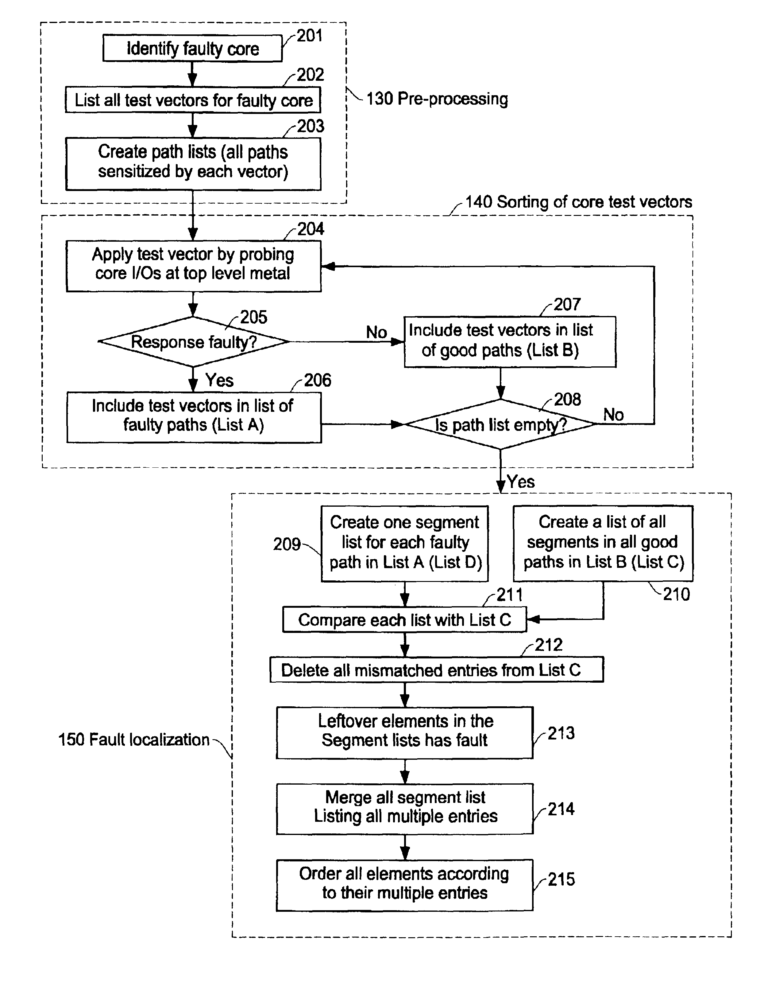
[0032]The present invention is now described in more detail with reference to the accompanying drawings. FIGS. 3-8 show the method of present invention for evaluating design integrity and fault diagnosis of embedded core based system-on-a-chip (SoC) ICs. FIGS. 3-5 show a special structure of SoC for testing the SoC and embedded cores therein in a silicon form (silicon debug) in accordance with the present invention. FIGS. 6-8 show the test procedures and test system structure for evaluating the SoC and embedded cores therein in the present invention. The method of the present invention is applicable only to the SoC that are designed to have the particular structure shown in FIGS. 3-5.

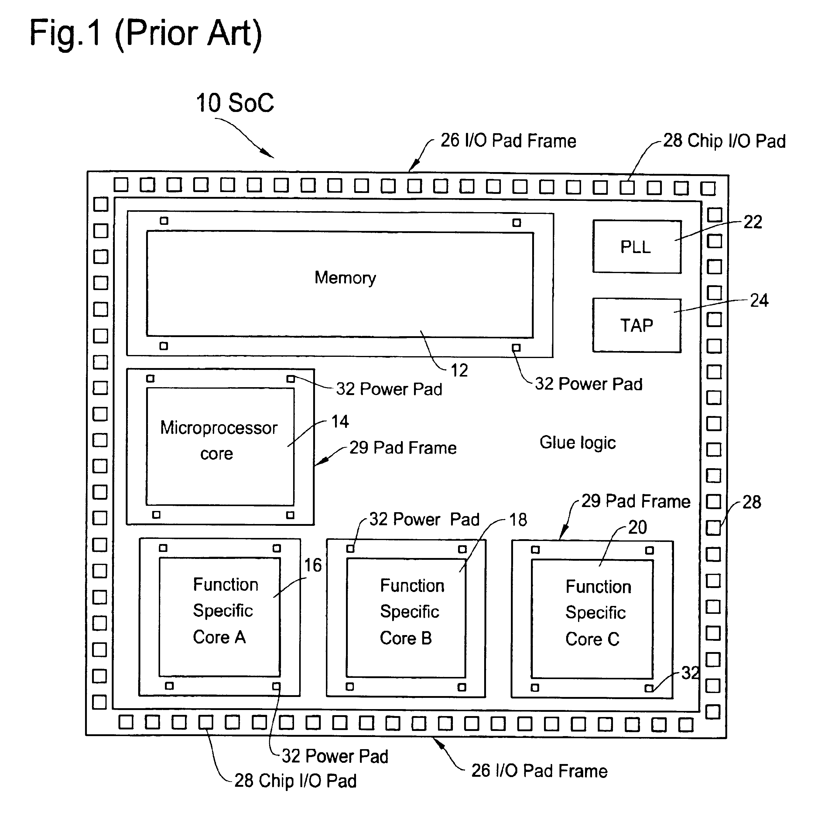
[0033]Referring now to FIGS. 3-5, there is shown a basic structure of an SoC to which the method of the present invention is implemented. This configuration establishes an I / O interface (I / O pads) for each core that can be directly accessible by traditional contact probes. The I / O interface of individua...


PUM


Abstract

A method of evaluating a core based SoC detects and localizes faults in the cores or interconnects between the cores with high accuracy and observability. The method includes the steps of building two or more metal layers to create core I/O pads having all I/O pads and power pads on a surface of the top metal layer of the pad frame of each core, testing the SoC as a whole by applying test vectors to the SoC through chip I/O pads and evaluating response outputs of the SoC, testing each core in the SoC by applying core specific test vectors to the core through the core I/O pads on the top metal layer of the core and evaluating response outputs of the core, and finding a location of a fault when the fault is detected when testing the SoC chip as a whole or when testing each of the cores.

Description

[0001]This is a continuation-in-part of U.S. application Ser. No. 09 / 853,999 filed May 12, 2001.FIELD OF THE INVENTION[0002]This invention relates to a method of testing semiconductor devices, and more particularly, to a method of evaluating design integrity and fault diagnosis of embedded core based system-on-a-chip (SoC) ICs in a silicon form (silicon debug) with high accuracy and observability.BACKGROUND OF THE INVENTION[0003]In recent several years, ASIC (Application Specific Integrated Circuit) technology has evolved from a chip-set philosophy to an embedded cores based system-on-a-chip (SoC). An SoC is an IC designed by stitching together multiple stand-alone VLSI designs (cores) to provide full functionality for an application. Namely, the SoCs are built using pre-designed models of complex functions known as “cores” (also known as Intellectual Property or IP) that serve a variety of applications. These cores are generally available either in high-level description language (...

Claims


Application Information

Patent Timeline
Patent Type & Authority Patents(United States)
IPC IPC(8): G01R31/3185G01R31/317G01R31/28H01L21/82H01L21/822H01L27/04
CPCG01R31/317G01R31/31704G01R31/31705G01R31/31724G01R31/3185G01R31/318508G01R31/318552G01R31/28H01L22/00H01L27/04
Inventor RAJSUMAN, ROCHITYAMOTO, HIROAKI
Owner ADVANTEST CORP
Why Eureka
Try Eureka