
Fiber optic field programmable gate array integrated circuit packaging

a technology of integrated circuits and fiber optics, applied in the field of fiber optic integrated circuit packages, can solve the problems of affecting the operation of fpga devices, and affecting the i/o of future fpga devices

Active Publication Date: 2005-09-20
XILINX INC
View PDF24 Cites 87 Cited by
  • Summary
  • Abstract
  • Description
  • Claims
  • Application Information

AI Technical Summary

Benefits of technology

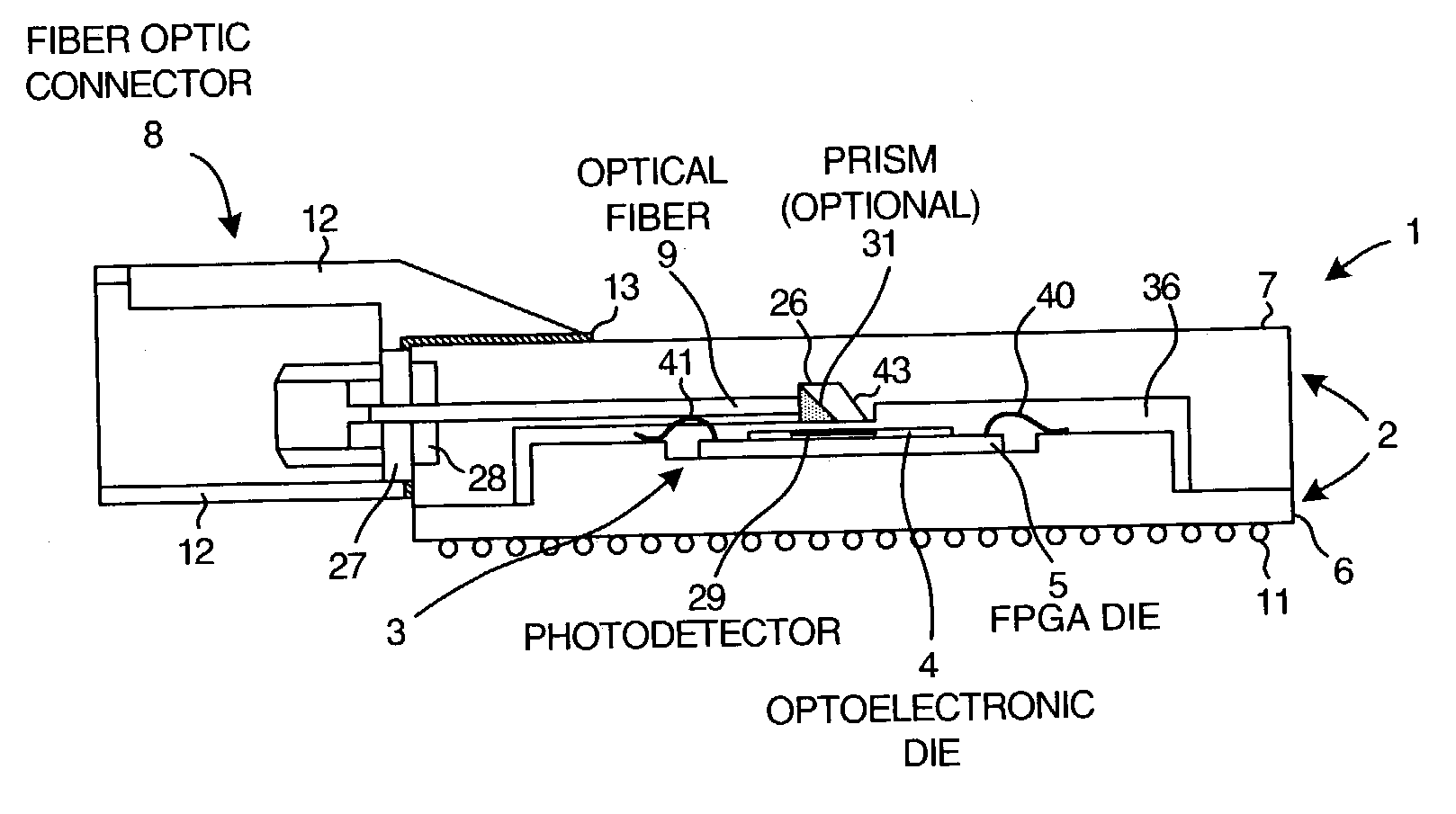
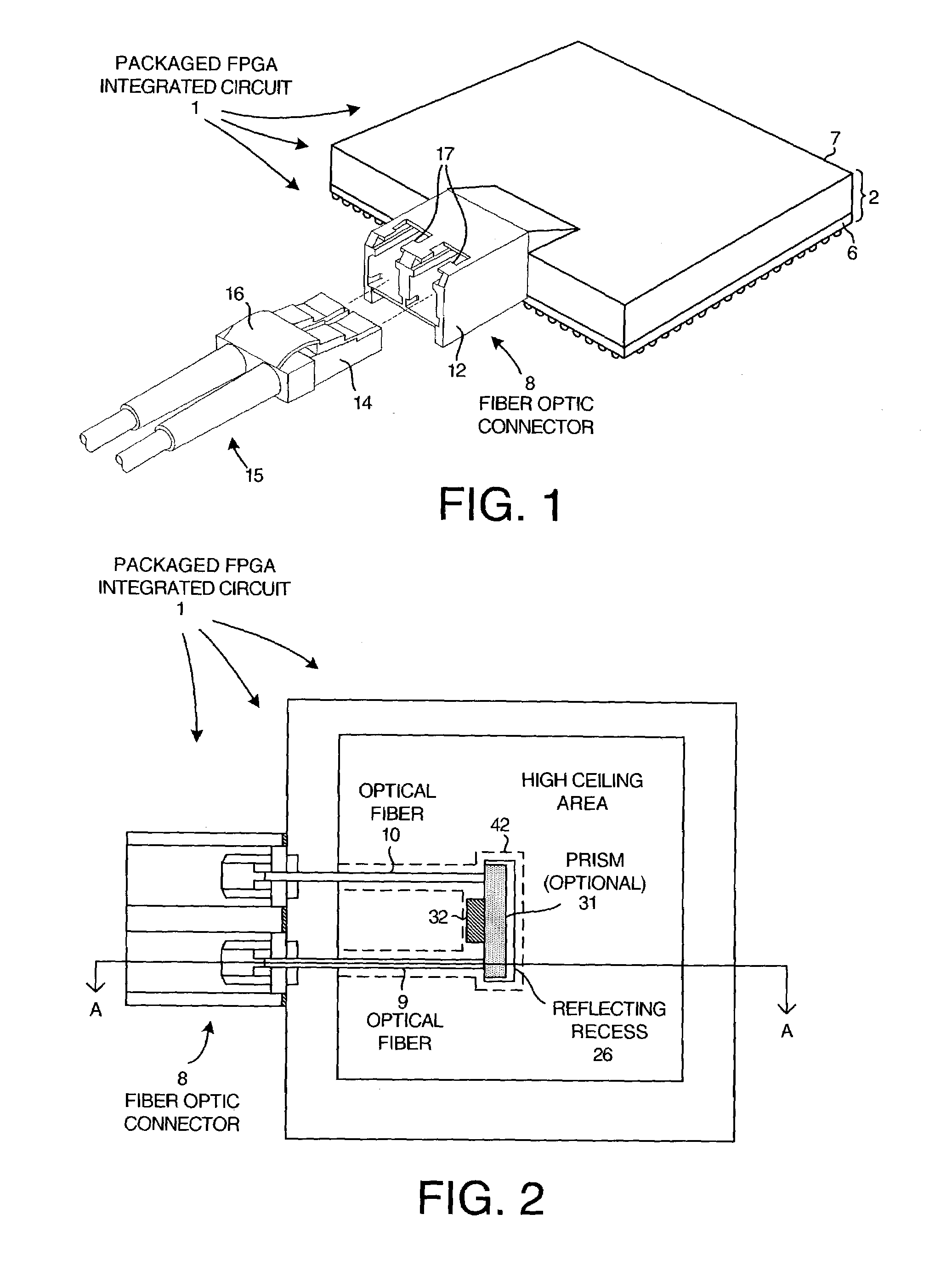
[0015]The packaged FPGA integrated circuit is advantageous in that it has a thin profile, low power consumption, and assembly-related advantages. These and other advantages are described in the detailed description below.
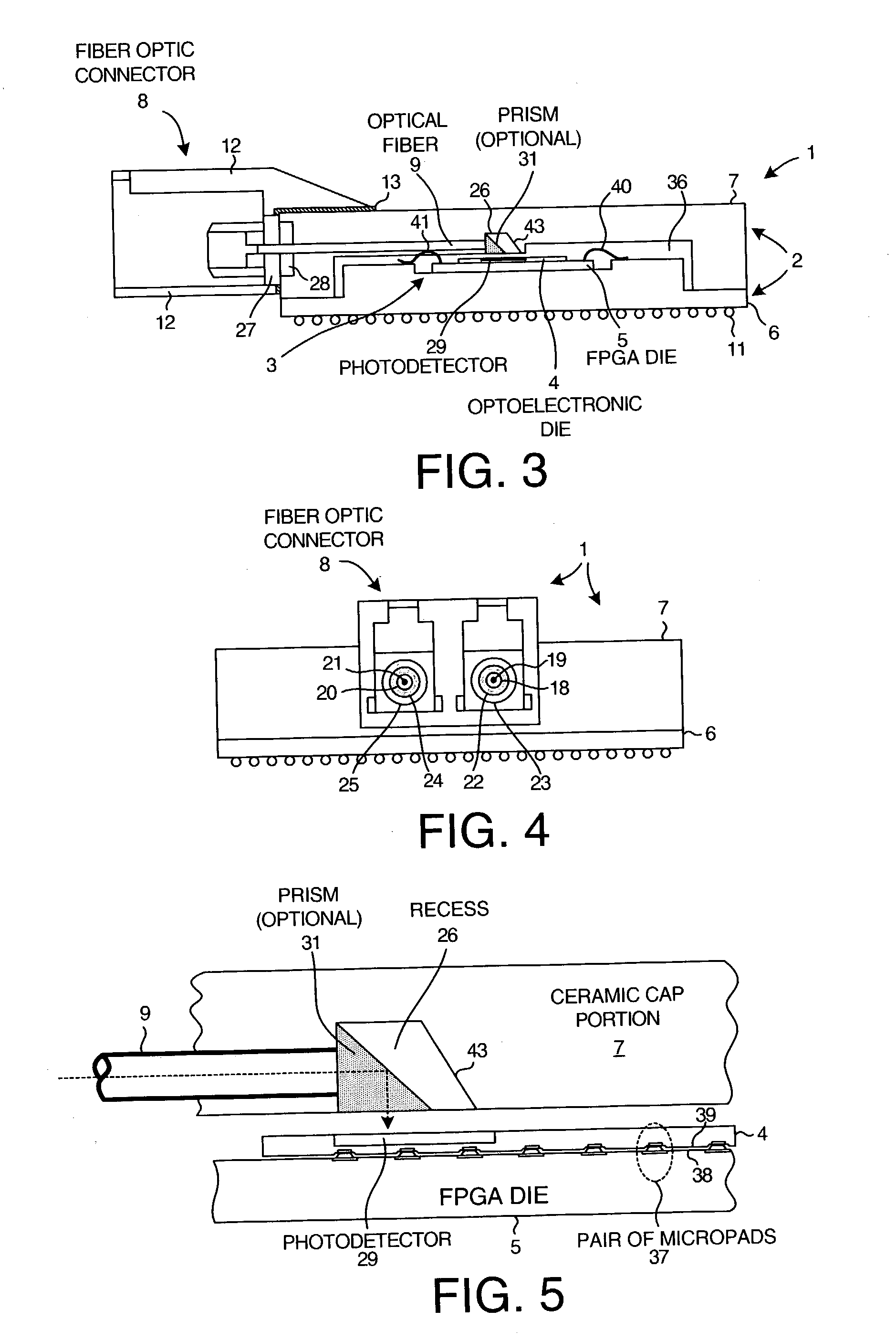
[0020]In a sixth embodiment, a micromirror device is fixed to the inside surface of the cap portion of the integrated circuit package. Electrical signal conductors extend from the FPGA die, through the base portion of the package, up through the cap portion of the package, and to the micromirror device so that the micromirror device is controlled by the FPGA die. An optical fiber is used to direct light from a fiber optic connector of the package, through the wall of the cap portion, and to the micromirror device. The micromirror device focuses or directs light exiting the optical fiber onto the photodetector of the optoelectronic die. Similarly, the micromirror device is usable to focus or direct light emitted from a light generating device of the optoelectronic die onto a second optical fiber used to communicate light out of the integrated circuit package. This allows for misalignments between the optical fibers, micromirror device, and / or the optoelectronic device.

Problems solved by technology

It is envisioned that soon many FPGA devices will be input / output (I / O) limited or the operation of the FPGA devices will be hampered by inadequate capacity to get information into and out of the FPGA package.
Future FPGA devices may be I / O limited both in terms of not having enough space at the periphery of the FPGA die to accommodate additional I / O functionality, and in terms of the speed of the on-chip I / O facilities being too slow to communicate the desired amount of information in the amount of time available.
High speed switching on these conductors in combination with the relatively large parasitic capacitance and inductances of these conductors results in an undesirably large amount of power consumption.
In addition to high power consumption, the design of the printed circuit board traces used to communicate information between these devices may be a daunting and time-consuming task for many FPGA users.
High speed printed circuit board design can involve complex considerations and problems.
In addition to the difficulties associated with high speed printed circuit board design, disposing each of the various devices in its own separate package increases the aggregate packaging cost involved in realizing the system.
The task of designing a great many high speed communication paths between the two FPGAs may be a difficult and time-consuming task.
If a complex multi-layer printed circuit board is used for this purpose, the communication paths realized as traces on the printed circuit board are inflexible.
The use of a printed circuit board to make large numbers of independent communication channels between such FPGAs is, therefore, be cumbersome.
Although the package disclosed in U.S. Pat. No. 6,364,542 may be suitable for certain applications, fabrication and assembly of the integrated circuit package may be restrictively complex.
If the clearance between the top of the integrated circuit die and the bottom inside surface of the package is too small, then the bond balls used to make contact with the integrated circuit may actually damage the integrated circuit die.
If the clearance is too great, then adequate and repeatable contact between the bond balls and the integrated circuit may not be made.
This assembly introduces undesirable assembly steps and testing steps.
Not only is the assembly process complex, but the bond balls and posts used to connect the integrated circuit die to the optoelectronic die are large in comparison to the size of transistors and conductor lines on the integrated circuit die.
Running high speed signals over the large bond balls and posts results in increased power consumption.

Method used


Image

  • Fiber optic field programmable gate array integrated circuit packaging
  • Fiber optic field programmable gate array integrated circuit packaging
  • Fiber optic field programmable gate array integrated circuit packaging

Examples


second embodiment

[0085]FIG. 21 is a cross-sectional diagram of a packaged FPGA integrated circuit 200 in accordance with the present invention. In this embodiment, light passing through a first optical fiber 201 from an LC SFF connector 202 is redirected by a bent first optical fiber 201 from a direction substantially parallel to the upper surface of FPGA die 5 to a direction substantially perpendicular to the upper surface of optoelectronic die 4. Although not shown in FIG. 21, light emitted from the light generating device of optoelectronic die 4 is redirected by a second bent optical fiber (not shown) ninety degrees from a direction substantially perpendicular to the upper surface of optoelectronic die 4 to the direction substantially parallel to the upper surface of FPGA die 5. The light from the light generating device is directed by the second optical fiber to a second ferrule and sleeve (not shown) of connector 202. The second ferrule and sleeve are disposed behind the ferrule and sleeve illu...

third embodiment

[0088]FIG. 22 is a cross-sectional diagram of a packaged FPGA integrated circuit 300 in accordance with the present invention. In this embodiment, an optical connector 301 is fixed to an upper cap portion 302 of the integrated circuit package. Cap portion 302 of the integrated circuit package can, for example, be made of ceramic, metal or polyimide. An optical fiber 303 extends downward in a direction substantially perpendicular to the upper surface of optoelectronic die 4 from connector 301, through cap portion 302, and to the upper surface of optoelectronic die 4. Optical connector 301 is shown as an ST bulkhead connector. In contrast to the embodiment of FIG. 21, the optical fiber 303 in the embodiment of FIG. 22 does not bend. As in the case of the embodiment of FIG. 21, the optical fiber can be made to touch the upper surface of optoelectronic die 4, or can be spaced so that its end is very close (about 5 microns) to the upper surface of optoelectronic die 4. By reducing the di...

fourth embodiment

[0089]FIG. 23 is a cross-sectional diagram of a packaged FPGA integrated circuit 400 in accordance with the present invention. In this embodiment, rather than the backside surface of an optoelectronic die being die-bonded to the upper surface of an FPGA die, an optoelectronic die 4 is mounted on the upper surface of FPGA die 5 such that the plane of the face side of the optoelectronic die 4 is oriented perpendicularly with respect to the plane of the upper surface of FPGA 5. Optoelectronic die 4 is thin. To facilitate mounting of such a thin die on its edge, a relatively thick support wafer is bonded to a wafer of optoelectronic dice. The composite wafer assembly is then sectioned into the relatively thick structures. Thick die structure 401 shown in cross-section in FIG. 23 is one such structure. Portion 402 is a portion of the support wafer. The thick die structure 401 is then mounted on its side on the upper surface of FPGA 5 as shown in FIG. 23. An optical fiber extends from con...


PUM


Abstract

An FPGA is readily connectable to a high-speed fiber optic link by snap fitting an external fiber optic cable into an accommodating duplex fiber optic connector of a low-profile packaged FPGA integrated circuit. The low-profile packaged FPGA integrated circuit includes a die-bonded assembly disposed within a co-fired multilayer ceramic integrated circuit package. The die-bonded assembly includes the optoelectronic die, the bottom surface of which is die-bonded and electrically interconnected by micropads to the upper surface of the core of an FPGA integrated circuit die. A first optical fiber communicates light from the connector, through the package, and to a photodetector on the optoelectronic die. A second optical fiber communicates light from a laser diode on the optoelectronic die, through the package, and to the connector. In some embodiments, a micromirror device is disposed within the package to redirect light between the optoelectronic die and the optical fibers.

Description

FIELD OF THE INVENTION[0001]The present invention relates to fiber optic integrated circuit packages.BACKGROUND INFORMATION[0002]As the amount of functionality built into field programmable gate arrays (FPGAs) increases and as electronic systems increase in throughput and signaling speed, the amount of information flowing into and out of FPGAs has increased. It is envisioned that soon many FPGA devices will be input / output (I / O) limited or the operation of the FPGA devices will be hampered by inadequate capacity to get information into and out of the FPGA package. Future FPGA devices may be I / O limited both in terms of not having enough space at the periphery of the FPGA die to accommodate additional I / O functionality, and in terms of the speed of the on-chip I / O facilities being too slow to communicate the desired amount of information in the amount of time available.[0003]FPGAs see increasing use in networking applications. A networking application may, for example, involve a prin...

Claims


Application Information

Patent Timeline
Patent Type & Authority Patents(United States)
IPC IPC(8): G02B6/42G02B6/38G02B6/43
CPCG02B6/3897G02B6/4214G02B6/4246G02B6/4292G02B6/43H01L2924/15311H01L2224/48091H01L2224/48227H01L2924/00014
Inventor CONN, ROBERT O.
Owner XILINX INC
Learn More