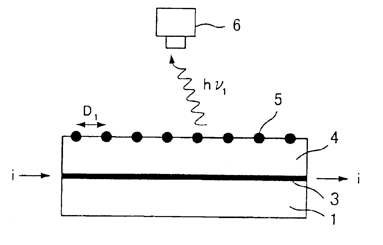
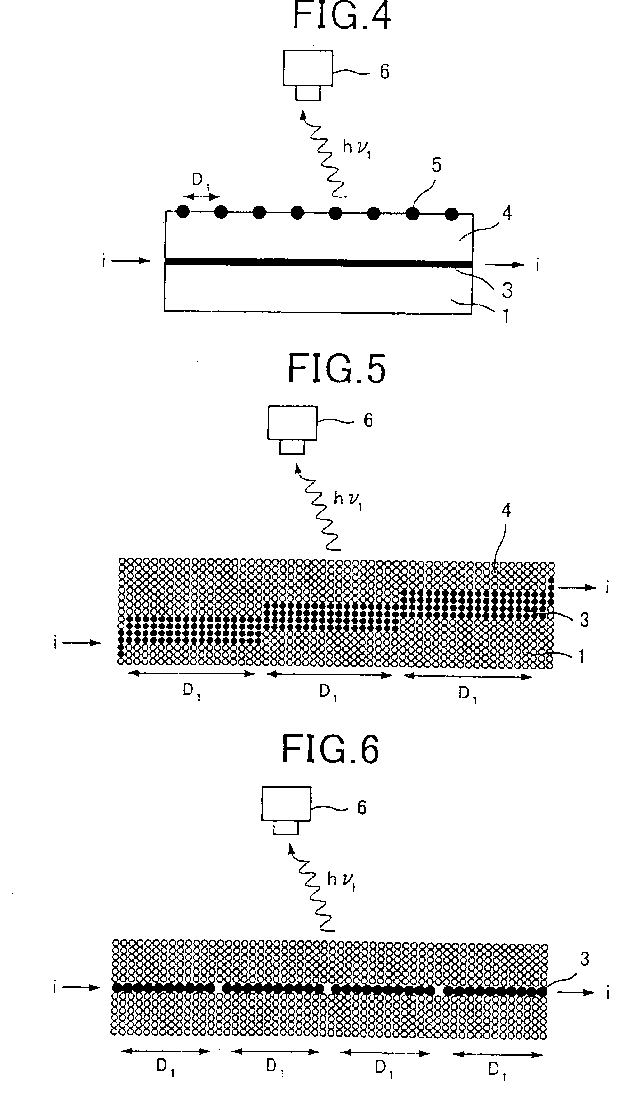
[0019]Volume plasmon in a three-dimensional solid matter and surface-plasmon or Mie plasmon in the vicinity of a three-dimensional solid matter are examples of three-dimensional plasmon. On the other hand, low-dimensional plasmon is originated in fluctuation of a charge density wave, which localizes in a two-dimensional plane or a one-dimensional structure.
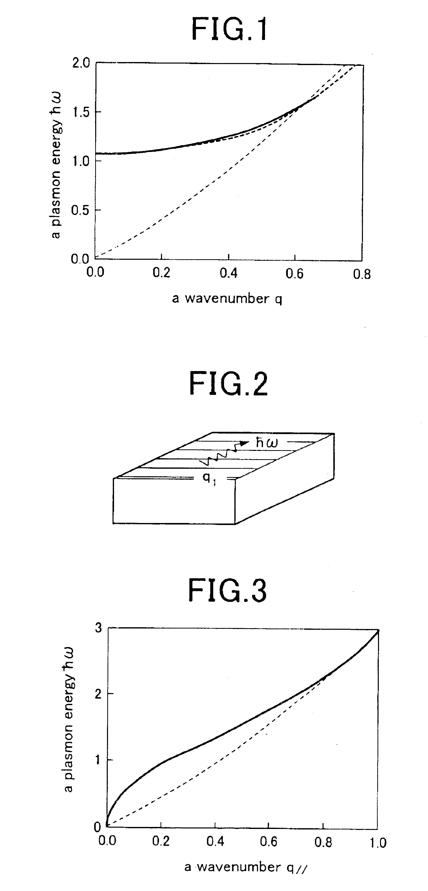
[0020]Dispersion of a plasmon frequency ωp(q) with respect to a wavenumber q of three-dimensional plasmon is represented by the below-mentioned formula, wherein ωp0 is a plasma frequency determined by carrier density N and effective mass m* of a solid matter, and α and β are constants, as disclosed in H. Raether, Excitation of plasmons and Interband Transitions by Electrons, Vol.88 of Springer Tracts in Modern Physics (Springer, Berlin, 1980) and Surface Science Reports 22 (1995) pp.1-71. ω p0 = ( 4 π ne 2 m * ) 1 / 2 ( CGS ) or ( 2 π ne 2 m * ) 1 / 2
[0021]a frequency of bulk-plasmon a frequency of surface-plasmon
ωp(q)=ωp0+αq+βq2+O(q3)
[0022]The vibration energy ωp is finite at q=0 and substantially deviates to a positive side with an increase of the wavenumber q. As a result, the vibration frequency ωp(q) is limited to the plasma frequency ωp0 at most. Plasmon is not generated due to Landau damping at a wavenumber q more than Fermi wavenumber qF of a substance. In short, three-dimensional plasmon has an energy close to the value of ωp0, as shown in FIG. 1.
[0023]On the other hand, low-dimensional plasmon that originated in a charge density wave localized in a one-dimensional structure or two-dimensional plasmon that originated in a charge density wave localized in a two-dimensional plane has a vibration energy distribution quite different from the three-dimensional plasmon. For instance, energy dispersion of two-dimensional plasmon between two dielectrics with dielectric functions ∈1, ∈2 approximated by the following formula, wherein N2D is two-dimensional carrier density, m* is effective carrier mass and is a component of a wavenumber in parallel to a two-dimensional surface structure, as disclosed in Phys. Rev. Lett. 18, pp. 546-548 (1967). ω 2 D ( q // ) 2 ≅ 4 π N 2 D ( ɛ 1 + ɛ 2 ) m * · q // + 3 ℏ 2 π N 2 D 2 m * 2 · q // 2 + O ( q // 3 )
[0024]The specified energy dispersion means that a plasmon energy can be generated over a broad range from a far-infrared region to an ultraviolet region by proper selection of a substance, which has two-dimensional carrier density N2D, effective carrier mass m* and permittivities ∈1, ∈2 each suitable for the purpose, as shown in FIG. 3.
[0025]One-dimensional plasmon has energy dispersion approximated by the following formula, wherein N1D is one-dimensional carrier density and a is a constant, as disclosed in Phys. Rev. B, pp. 1936-1946 (1996). Therefore, a plasmon energy is generated over a broad range from a far-infrared region to an ultraviolet region by proper selection of a substance.
ω1D(q)2=αN1Dqz,900·√{square root over (|ln|q ∥)}
[0026]The energy of the low-dimensional plasmon is varied from zero to a large extent as a function of plasmon momentum, as mentioned above. However, a dispersion relation of the low-dimensional plasmon does not cross a dispersion relation of an electromagnetic wave except for zero energy. Therefore, the plasmon energy can not be converted to a luminescent energy under normal conditions.
[0027]In this regard, a periodic nanostructure is incorporated inside or in the vicinity of a low-dimensional conductive structure, in order to enhance combination of plasmon with light, resulting in production of plasmon luminescence. The periodic nanostructure in this specification means a structure, which has a periodicity corresponding to a real space periodicity D1(=2π/q1), wherein a wavenumber q1 gives a specified luminescent energy (h/2π)ω1 in a wavenumber-energy curve of low-dimensional plasmon.
[0028]A periodic structure 5 (FIG. 4), which is incorporated in a surface layer of or inside dielectrics 1 and 4 by nano-fabricating, or periodic structures (FIGS. 5 and 6), which are incorporated in a low-dimensional conductive structure 3 at an interface between dielectrics 1 and 4, are suitable for the purpose. The periodic nanostructure 5 or the low-dimensional conductive structure 3 with the periodic nanostructure has a pattern unit repeated with a predetermined pitch D1. Plasmon momentum q1 capable of coupling with an electromagnetic wave is controlled by the periodic pattern with the pitch D1. Consequently, luminescence with a predetermined energy (h/2π)ω1 or hν1 is produced by selectively coupling plasmon, which has an energy (h/2π)ω1 corresponding to predetermined plasmon momentum, with light.
[0029]An energy is inputted to low-dimensional plasmon by charging carriers of a low-dimensional structure with a direct or alternative electric field, i.e. input of a direct or alternative current i, and the electric energy is converted to luminescence with a predetermined energy (h/2π)ω1. The line width of the emission spectrum can be narrowed by improving accuracy of the pitch D1, thus reducing defect density in a crystal and soon.
[0030]Low-dimensional conductive structures are representatively listed below: [0031] (a) A space-charge layer or a quantum well, which is formed on a surface or interface of a semiconductor or dielectric for storage of carriers. [0032] (b) A surface or interfacial electronic band with high carrier density, which is formed on a surface or heterojunction of a semiconductor or dielectric. [0033] (c) A δ-doped layer with high carrier density, which is formed inside a semiconductor or dielectric. [0034] (d) A one-dimensional structure, which has a confinement structure nano-fabricated in a two-dimensional structure such as a space-charge layer or a quantum well along a planar direction. [0035] (e) A low-dimensional conductive structure with high density, which is formed in a conductive organic molecule, a conductive polymer, an oxide superconductor and other organic substances with one- or two-dimensional structures.
[0036]The low-dimensional conductive structures (b), (c) and (e) allow presence of plasmon with thickness similar to a monolayer, so that a periodic nanostructure is incorporated in a atomic sized structural body. As a result, a solid light-emitting element, which produces luminescence over a broad range from a far-infrared region to an ultraviolet region, can be fabricated in a size from sub-nanometer to several hundreds of nanometer scale.
[0037]The following structures (A) to (C) may be used for coupling low-dimensional plasmon, which consists in the low-dimensional conductive structure, with light. [0038] (A) A periodic structure 5 (FIG. 4), which is constructed from fine metallic wires, grooves or dots formed on a dielectric layer 4 in the vicinity of a low-dimensional conductive structure by nano-fabricating, e.g. masked deposition, focused ion-beam processing or electron-beam lithography. [0039] (B) A low-dimensional conductive structure, which has a periodic nanostructure incorporated therein by selection of a template substrate suitable for growth of a film and self-organization of the film during growth. A low-dimensional conductive structure 3 (FIG. 5) with regular array of steps, which are formed by growth of a film on slightly inclined surfaces (i.e. surfaces with atomic steps), belongs to this group. [0040] (C) A periodic structure (FIG. 6), which is self-organized during epitaxial growth or polymerization of an organic molecule or polymer. A periodic structure, which is formed inside a conductive polymer synthesized by such the manner that functional groups as a scattering center are periodically arranged, belongs to this group.
[0041]Especially, incorporation of the periodic structure (B) or (C) with steps similar to height of a monolayer in the low-dimensional conductive structure (b), (c) or (e), wherein plasmon exists with thickness similar to the monolayer, is effective for enhancing combination of the plasmon with light.
[0042]Other features of the present invention will be clearly understood from the following Example, referring to the drawings.
[0043]Ag was deposited as a monolayer on a (111) surface of Si to prepare a surface structure of Si(111)−√{square root over ( )}3×√{square root over ( )}3−Ag. The surface structure was irradiated with low-speed electron beam of impact energy of −5.8−50.5 eV. An energy and a frequency of two-dimensional plasmon were measured by energy loss spectrum.
[0044]Measured results are shown in FIG. 7. It is noted from FIG. 7 that plasmon was produced over a broad energy range of 0-520 meV under conditions of ∈1=1, ∈2=∈si=11.5, N2D=1.9×10¹³/cm2, m*=0.3me (me is mass of free electron). Greater plasmon energy was generated in case of a low-dimensional substance, which had small dielectric functions ∈1, ∈2 and small effective mass m* but high two-dimensional carrier density N2D. The results prove that a light emitter, which can produce luminescence with an energy over a broader range, can be fabricated.
[0045]A luminescent energy of (h/2π)ω1 or hν1 can be generated by a periodic nanostructure, which has a periodicity D1(=2π/q1), wherein a wavenumber q1 gives a plasmon energy of (h/2π)ω1 or hν1 in a wavenumber-energy curve. Due to the periodic microstructure, plasmon is surely coupled with an electric field accompanying the structure, so as to produce luminescence of (h/2π)ω1 or hν1. The produced luminescence is detected by a photodetector 6.
[0046]A low-dimensional plasmon-light emitter according to the present invention as mentioned above has a periodic nanostructure incorporated inside or in the vicinity of a low-dimensional conductive structure, which generates low-dimensional plasmon. Since low-dimensional plasmon is strongly combined with light due to incorporation of the periodic nanostructure, an inputted electric energy can be converted to luminescence with an arbitrary energy over a broad range from a far-infrared region to an ultraviolet region. Consequently, the plasmon-light emitter is useful as sensors, display devices and light-emitting elements in various fields.