High holding voltage ESD protection structure and method

a protection structure and high holding voltage technology, applied in the direction of diodes, transistors, semiconductor/solid-state device details, etc., can solve the problems of not only large ggnmos devices, damage to analog circuits, and over-voltage handling capabilities of analog circuits, so as to reduce the size of p+ emitters, increase the value of holding voltage, and high holding voltage

Inactive Publication Date: 2005-09-20
NAT SEMICON CORP
View PDF2 Cites 13 Cited by
  • Summary
  • Abstract
  • Description
  • Claims
  • Application Information

AI Technical Summary

Benefits of technology

[0031]The present invention provides an ESD protection structure with a high holding voltage suitable, among other things, for CMOS I / O and power supply protection. In particular, it provides a low-voltage triggering silicon-controlled rectifier-like (LVTSCR-like) device that increases the value of the holding voltage by reducing the size of the p+ emitter of the device. The invention also provides for a high holding voltage device that supports high current densities by keeping the p+ below a certain size and increasing n+ emitter to limit space charge neutralization, and a method of manufacturing such a device.
[0036]Further, according to the invention, there is provided a LVTSCR-like device having a reduced p+ emitter region. The reduced p+ emitter region reduces the number of holes for space charge neutralization. Thus, it reduces the total emitter injection current and provides only partial injected space charged neutralization. The uncompensated space charge effects the electric field distribution in the device which causes a higher voltage drop. Although the modified structure reduces the current density that the device will support, the maximum current after triggering of the proposed structure is, nevertheless, 3–5 times more than in the case of traditional GGNMOS.

Problems solved by technology

Analog circuits typically display sensitivity to excessive voltage levels.
Transients, such as electrostatic discharges (ESD) can cause the voltage handling capabilities of the analog circuit to be exceeded, resulting in damage to the analog circuit.
One of the difficulties encountered in designing such protection circuitry is that the specifications for these clamps have to fit within a relatively small design window that, on the one hand, must take into account the breakdown voltage of the circuit being protected, and, on the other hand, avoid latch-up under normal operation.
However, GGNMOS devices are not only large, consuming a lot of space on a chip, they also suffer from the disadvantage that they support only limited current densities.
One of the disadvantages of SCR 100, however, is that a very large positive voltage, e.g., 50 volts, must be dropped across nodes 120 and 126 before the junction between p-type material 110 and n-well 112 breaks down.
As a result, SCR 100 can not be used to protect devices, such as MOS transistors, that can be permanently damaged by much lower voltages, e.g., 15 volts.
However, one disadvantage of LVTSCR 200, and, for that matter, any SCR is that it suffers from a holding voltage that is often less than the minimum (or latch-up) voltage of the ESD protection window.
As a result, standard LVTSCRs are >unattractive candidates for providing ESD protection to power supply pins.
Thus, in spite of higher current availability from an LVTSCR after snap back, conventional CMOS integrated circuits are usually protected by grounded gate NMOS snap back structures (GGNMOS) due to the latch-up limitations of LVTSCRs.

Method used


Image

  • High holding voltage ESD protection structure and method
  • High holding voltage ESD protection structure and method
  • High holding voltage ESD protection structure and method

Examples


Embodiment Construction

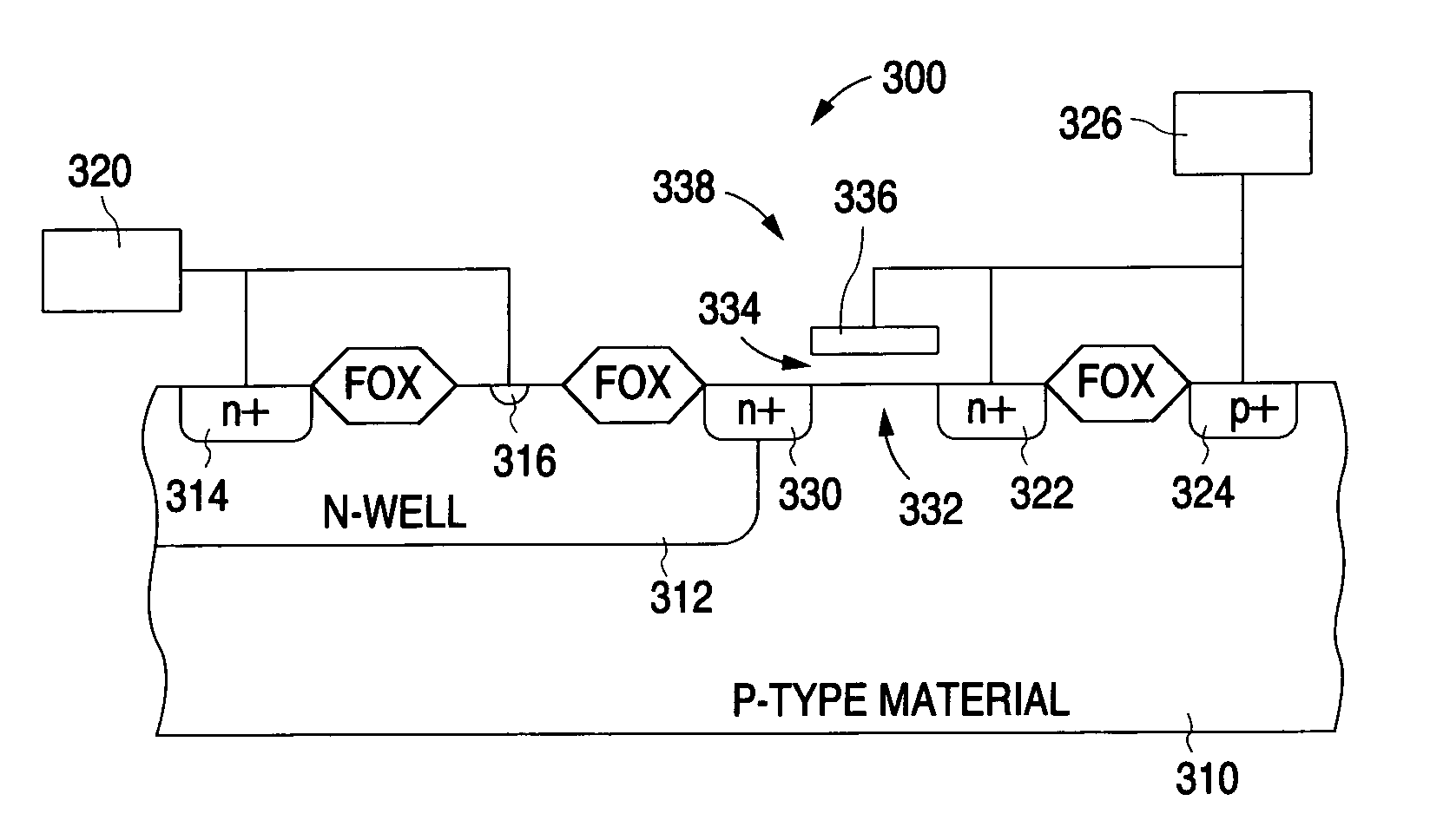
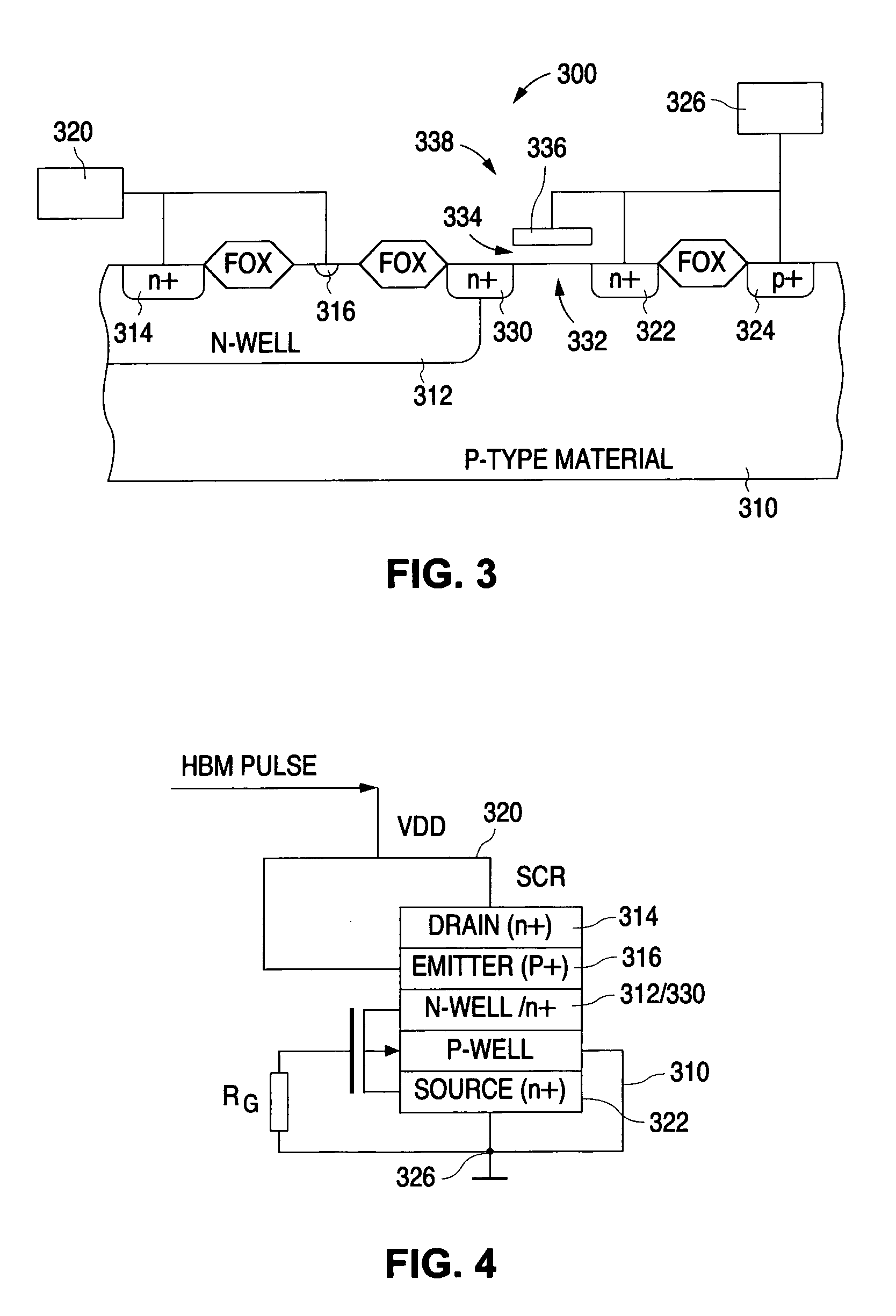
[0045]In order to achieve a structure having improved holding voltage characteristics than a LVTSCR and improved current density than a GGNMOS the present invention proposes using a device having the features of a SCR or LVTSCR, but wherein the dimensions of the features are changed over that of a standard LVTSCR, to achieve reduced space charge neutralization.

[0046]FIG. 3 shows a cross-sectional view that illustrates on embodiment of a LVTSCR-like device 300 in accordance with the present invention. As described in greater detail below, the holding voltage of the device 300 is increased by reducing the space charge neutralization, which is achieved by limiting the number of holes injected into the device. This, in turn, is achieved by reducing the p+ emitter junction area defined by the device 300. As shown in FIG. 3, the p+emitter of the pnp transistor of device 300 is reduced in size as compared to the conventional p+emitter 116 shown in FIG. 2.

[0047]As shown in FIG. 3, device 30...


PUM


Abstract

The holding voltage (the minimum voltage required for operation) of a LVTSCR-like device is increased to a value that is greater than a dc bias on a to-be-protected node. The holding voltage is increased by reducing the size of the p+ emitter defined by the LVTSCR-like device. As a result, the LVTSCR can be utilized to provide ESD protection to power supply pins, having better current capabilities than a GGNMOS and better holding voltage characteristics than a LVTSCR.

Description

FIELD OF THE INVENTION[0001]The present invention relates to a high holding voltage ESD protection device, and more particularly, to a device displaying good current capabilities.BACKGROUND OF THE INVENTION[0002]Analog circuits typically display sensitivity to excessive voltage levels. Transients, such as electrostatic discharges (ESD) can cause the voltage handling capabilities of the analog circuit to be exceeded, resulting in damage to the analog circuit. Clamps have been devised to shunt current to ground during excessive voltage peaks.[0003]One of the difficulties encountered in designing such protection circuitry is that the specifications for these clamps have to fit within a relatively small design window that, on the one hand, must take into account the breakdown voltage of the circuit being protected, and, on the other hand, avoid latch-up under normal operation. Thus, the clamp must be designed such as to be activated below the breakdown voltage of the circuit that is to ...

Claims


Application Information

Patent Timeline
Patent Type & Authority Patents(United States)
IPC IPC(8): H01L29/66H01L29/74H01L27/02
CPCH01L27/0262H01L29/7436H01L29/87
Inventor VASHCHENKO, VLADISLAVCONCANNON, ANNHOPPER, PETER J.
Owner NAT SEMICON CORP
Why Eureka
Try Eureka