Semiconductor device tester

Inactive Publication Date: 2005-09-20
KK TOPCON
View PDF51 Cites 22 Cited by
  • Summary
  • Abstract
  • Description
  • Claims
  • Application Information

AI Technical Summary

Benefits of technology

[0016]An object of the present invention is to further improve the technique for detecting a substrate current produced by irradiation of electron beam to thereby

Problems solved by technology

When a parallel electron beam is used, focal distance becomes infinite so that focus regulation becomes u

Method used


Image

  • Semiconductor device tester
  • Semiconductor device tester
  • Semiconductor device tester

Examples


first embodiment

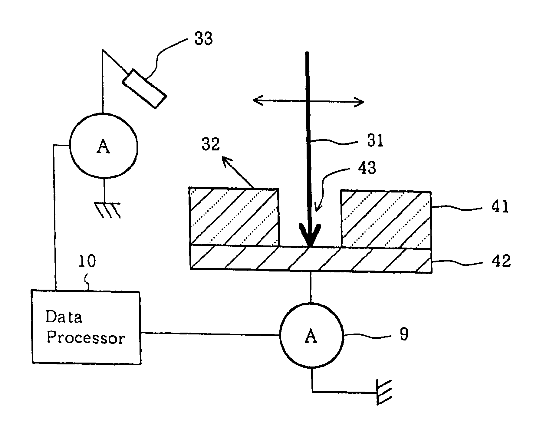
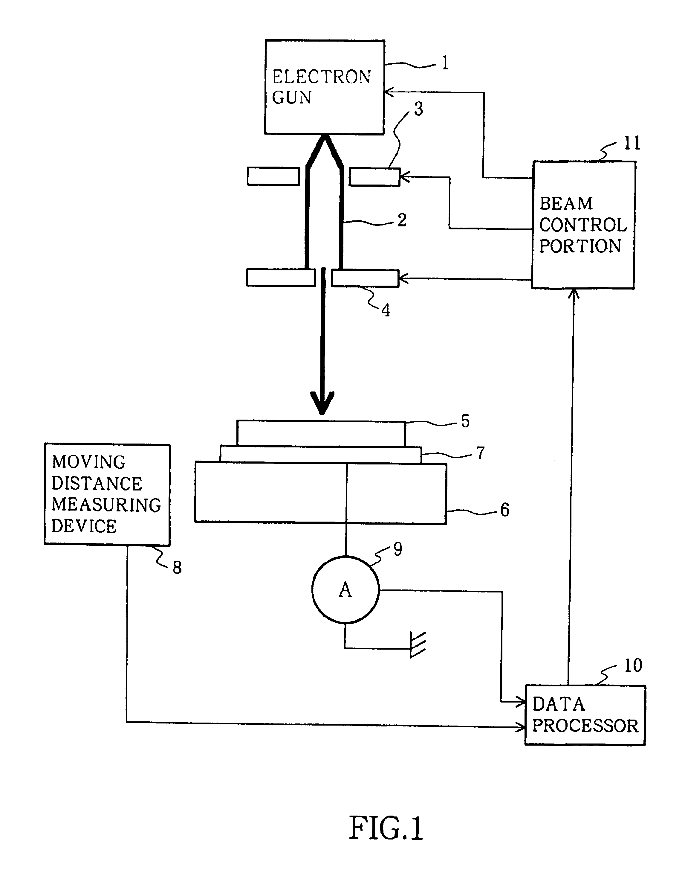
[0120]FIG. 1 is a block diagram showing a construction of a semiconductor device tester according to the present invention. The semiconductor device tester includes an electron gun 1 for generating electron beam 2, a condenser lens 3 and an aperture plate 4, which collimates the electron beam 2, a movable stage 6 for scanning irradiating positions of a sample 5 with electron beam by moving the sample 5, an electrode 7 and an ammeter 9, which measures current produced in the sample 5 by irradiation of electron beam 2, a moving distance measuring device 8 for measuring a moving distance of the movable stage 6, a data processor 10 such as a computer processing data resulting from the ammeter 9 and a beam control portion 11 for performing controls such as change of acceleration voltage of electron beam and / or change of irradiation period.

[0121]Electron beam 2 emitted from the electron gun 1 is once collimated to parallel beam by the condenser lens 3 and directed to the aperture plate 4 ...

second embodiment

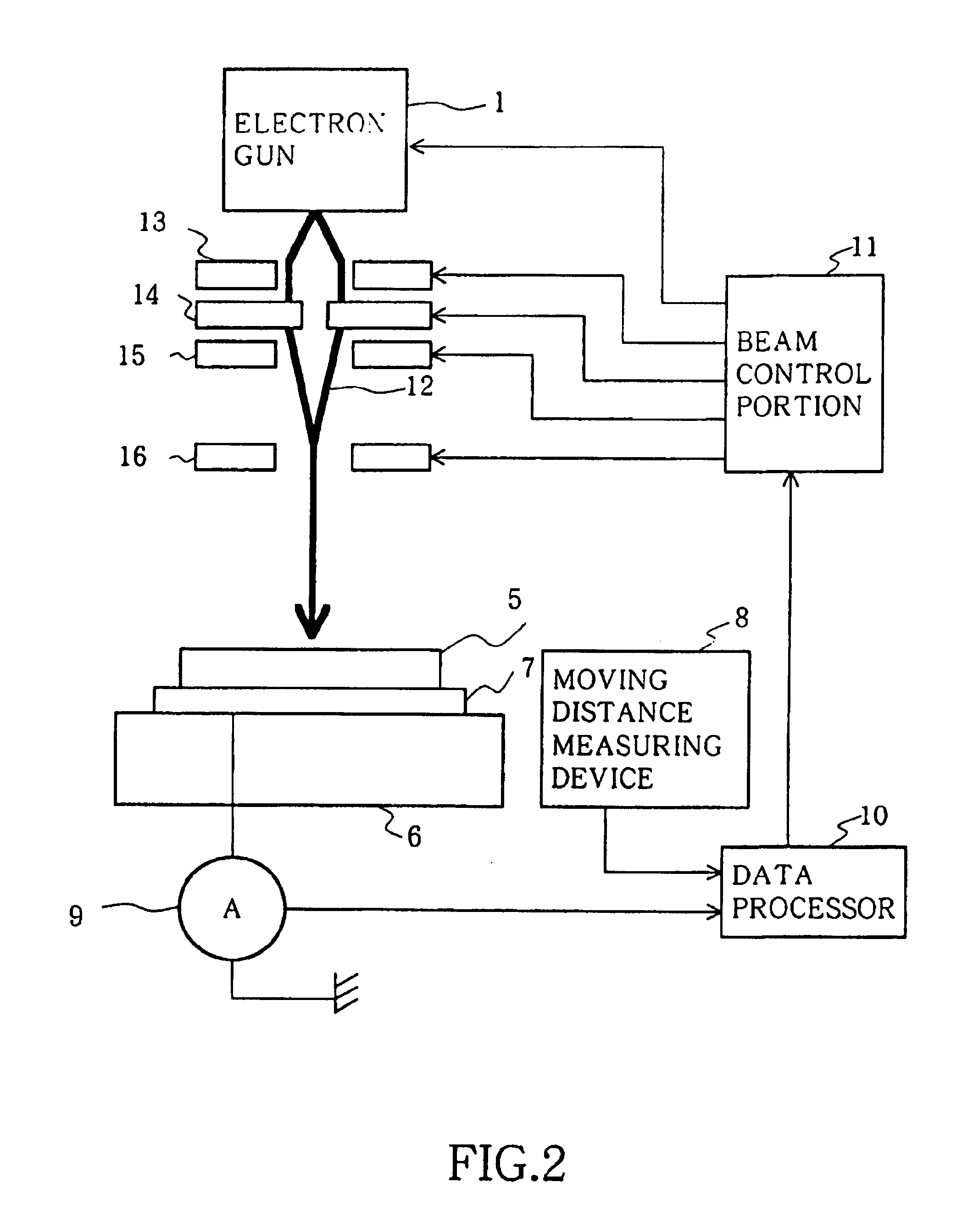
[0129]FIG. 2 is a block diagram of a semiconductor device tester according to the present invention, which is suitable when a cross sectional area of electron beam is on the order of a micron. In this tester, an electron beam generation system includes an afocal system composed of a second condenser lens 15 and an objective lens 16 and constitutes an electron optics system for converting incident parallel beam into parallel beam having cross sectional area smaller than an aperture area of an aperture plate 14.

[0130]That is, electron beam 12 emitted from the electron gun 1 is converted into parallel beam by the first condenser lens 13 and, then, converted into thin parallel beam by the aperture plate 14. Thereafter, the thin parallel beam is converged by the second condenser lens 15 and directed to the objective lens 16. In this electron beam generating system, the final beam, which is used to irradiate the sample 5, is formed without using the aperture of the aperture plate. Therefo...


PUM


Abstract

In one aspect, the present invention is a system and method for obtaining information regarding one or more contact holes and/or vias on a semiconductor wafer. In this regard, in one embodiment, the system comprises an electron gun to irradiate an electron beam on the one or more contact holes and/or vias wherein the electron beam includes a cross-section which is greater than the one or more contact holes. The system further includes a current measuring device, coupled to the semiconductor wafer, may measure a compensation current, wherein the compensation current is generated in response to the electron beam irradiated on the one or more contact holes. The system also includes a data processor, coupled to the current measuring device, to determine information relating to the one or more contact holes and/or vias using the compensation current.

Description

CROSS REFERENCE TO RELATED APPLICATIONS[0001]This application is a divisional application of application Ser. No. 09 / 702,831 (now U.S. Pat. No. 6,768,324), filed Nov. 1, 2000, which claims the benefit of priority, under 35 USC § 119, to Japanese Patent Application Nos. 11-315320, 2000-191817 and 2000-311196, filed on Nov. 5, 1999, Jun. 26, 2000 and Oct. 11, 2000, respectively, the contents of which are incorporated herein by reference.BACKGROUND OF THE INVENTION[0002]1. Field of the Invention[0003]The present invention relates to a semiconductor device tester using electron beam and, particularly, to a semiconductor device tester in which current flowing through a semiconductor device irradiated with electron beam is measured.[0004]2. Description of Related Art[0005]In a semiconductor device such as memory, contact-holes or via-holes are usually provided for electrically connecting active elements formed in a lower portion thereof to a wiring layer formed in an upper portion thereof...

Claims


Application Information

Patent Timeline
IPC IPC(8): G01R31/02G01R31/305G01R31/28G01B15/00G01B15/04G01B15/08G01N23/225G01N27/00G01R31/307G04B15/00H01J37/20H01J37/28H01L21/66
CPCG01R31/307H01J37/256H01J2237/20228H01J2237/221H01J2237/24564H01L22/00
Inventor YAMADA, KEIZOITAGAKI, YOUSUKEUSHIKI, TAKEOTSUJIDE, TOHRU
Owner KK TOPCON
Why Eureka
Try Eureka