Current sense amplifier

a current sense amplifier and amplifier technology, applied in amplifiers with semiconductor devices/discharge tubes, dc-amplifiers with dc-coupled stages, instruments, etc., can solve the problems of insufficient cell current for memory cells, difficult to read memory cells, and inability to provide memory cells with enough cell current, so as to increase the performance and speed of reading information stored in memory devices, improve the effect of performance and speed

Inactive Publication Date: 2005-09-20
IBM CORP +1
View PDF20 Cites 62 Cited by
  • Summary
  • Abstract
  • Description
  • Claims
  • Application Information

AI Technical Summary

Benefits of technology

[0014]Embodiments of the present invention achieve technical advantages as a current sense amplifier that is particularly useful in sensing current in resistive memory devices. A symmetrical high-speed current sense amplifier is disclosed that comprises complementary reference cells and configurable sensing paths that eliminate architecture-related capacitive mismatch contributions. The current sense amplifier is adapted for use in a symmetric sensing architecture, and includes at least one current mirror that may be configured using switching transistors, or a multiplexer may be used to select the input signal that is connected to the first or second side of the current mirror.
[0019]Advantages of embodiments of the present invention include increased performance and speed in reading information stored in memory devices. Capacitive load devices may be used to increase performance and balance capacitive loads. The configurable current mirror may be achieved by using select transistors, or a multiplexer may be used to select the input signal that is connected to the first or second side of the current mirror. In one embodiment, one of two transistors of the current mirror is selectable to function as a transistor diode. In another embodiment, the transistors of the current mirror are hard-wired but the input signal that is connected to the first or second side of the current mirror is selected by a multiplexer in the sense amplifier input path.

Problems solved by technology

This makes MRAM cell sensing more difficult.
The memory cell may not be able to provide enough cell current to discharge or charge a large bitline capacity within a required time.
This results in an excessive amount of time being required to read the memory cells.
Therefore, voltage sensing is not a preferred choice of sensing scheme for some memory devices, such as MRAM devices.

Method used


Image

  • Current sense amplifier
  • Current sense amplifier
  • Current sense amplifier

Examples


first embodiment

[0069]The cascode sense amplifier 40 design is advantageous in that the capacitive behavior is improved; therefore, the cascode sense amplifier 40 may provide some speed advantages. As in the first embodiment, the configurable current mirror 36 is advantageous because two current sense amplifiers 36 may be connected together, and the reference cell currents can be averaged.

[0070]Referring to FIG. 7, a capacitive load asymmetry within the current sense amplifier will be described. When transistor T5 is configured as a transistor diode, the capacitive load at the drain of T5 comprises the load due to the drain of T5, the gate of transistor T5 (via the connection by transistor T7), and also the gate load of transistor T6. The capacitive load at the drain of T6 comprises the load due to the drain of T6, no gate load because transistor T8 is not activated, and a small amount of drain load from T8. Therefore, there still remains a small amount of asymmetry of capacitance within the config...

embodiment 166

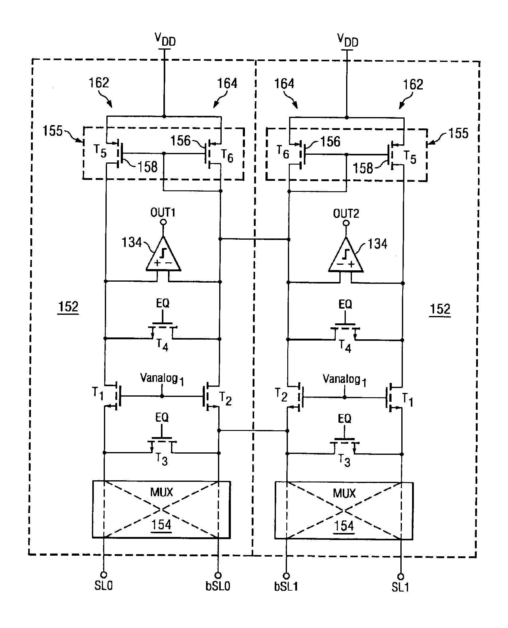
[0077]In FIG. 8, the multiplexer 154 adds resistance to the sensing path of the sense amplifier, which may reduce the sensed signal and may require a larger multiplexing device 154. To solve this problem, the multiplexer 160 may be disposed between the clamping devices T1 and T2 and the voltage comparator 134, as shown in the sense amplifier embodiment 166 of FIG. 9. This embodiment of the sense amplifier 166 is advantageous because a smaller multiplexer 160 may be used, and the sense signal is not reduced as much. As in the other embodiments, an equalizing transistor T3 may be coupled between the first input signal and the second input signal, and an equalizing transistor T4 may be coupled between the inputs of the voltage comparator, as shown. When used in a symmetric sensing architecture, preferably two or more current sense amplifiers 166 are utilized as a current sensing circuit, as described for the embodiment shown in FIG. 8.

[0078]In another embodiment 168 of the invention, t...

embodiment 168

[0079]Preferably, if signal V1 is on, then signal V2 is 0. Similarly, if signal V2 is on (or high) then signal V1 is 0. V1 and V2 are reference voltages and are preferably analog. For example, V1 and V2 may be Vanalog1 (see description for FIG. 6) or 0 V. A circuit (not shown) may be utilized to switch signals V1 and V2 to Vanalog1 or 0. This embodiment 168 is advantageous in that no additional multiplexing devices are required. An equalizing transistor T3 may be coupled between the first input signal SL0 and the second input signal bSL0, and an equalizing transistor T4 may be coupled between the inputs of the voltage comparator, as shown. As in the other hard-wired current mirror embodiments 152 and 166, when used in a symmetric sensing architecture, preferably two or more current sense amplifiers 168 are utilized as a current sensing circuit.


PUM


Abstract

A symmetrical high-speed current sense amplifier having complementary reference cells and configurable load devices that eliminates architecture-related capacitive mismatch contributions. The current sense amplifier is adapted for use in a symmetric sensing architecture and includes a configurable load device. The current sense amplifier includes a voltage comparator, a first clamping device coupled between a first input of the voltage comparator and a first input signal, the first clamping device being coupled to a reference voltage. A second clamping device is coupled between the second input of the voltage comparator and a second input signal, the second clamping device being coupled to the reference voltage. The load device may comprise a current mirror that is coupled between the first and second input of the voltage comparator. The current mirror may be configurable by select transistors. Alternatively, the load device may be a hard-wired current mirror, and a multiplexer may be used to select whether the first input signal or the second input signal is connected to a first or second side of the current mirror. Configurable dummy loads may be added at appropriate nodes to optimize the capacitive load and increase the speed of the amplifier. Equalization devices may be coupled between the first and second inputs of the voltage comparator, and between the first input signal and the second input signal.

Description

[0001]This invention was made with U.S. Government support under MDA972-99-C-0009 awarded by the Defense Advanced Research Projects Agency (DARPA). The U.S. Government has certain rights in this invention.TECHNICAL FIELD[0002]Embodiments of the present invention relate generally to semiconductor memory devices, and more particularly to sensing circuits for determining the resistive state of memory cells.BACKGROUND[0003]Semiconductors are used in integrated circuits for electronic applications, including radios, televisions, cell phones, and personal computing devices, as examples. One type of semiconductor device is a semiconductor storage device, such as a dynamic random access memory (DRAM) and flash memory, which uses a charge to store information.[0004]Spin electronics, which combines semiconductor technology and magnetics, is a more recent development in semiconductor memory devices. The spin of an electron, rather than the charge, is used to indicate the presence of a “1” or “...

Claims


Application Information

Patent Timeline
Patent Type & Authority Patents(United States)
IPC IPC(8): G11C7/06
CPCG11C7/067G11C2207/063
Inventor GOGL, DIETMARREOHR, WILLIAM ROBERTDEBROSSE, JOHN KENNETH
Owner IBM CORP
Why Eureka
Try Eureka