Apparatus and method for providing a signal port in a polishing pad for optical endpoint detection

a technology of optical endpoint detection and signal port, which is applied in the field of semiconductor manufacturing, can solve the problems of device failure, poor yield, environment in the gap , etc., and achieve the effect of constant environmen

Inactive Publication Date: 2005-10-11
APPLIED MATERIALS INC
View PDF12 Cites 35 Cited by
  • Summary
  • Abstract
  • Description
  • Claims
  • Application Information

AI Technical Summary

Benefits of technology

[0015]In still another embodiment, a method for minimizing interference during the in-situ thickness measurement of a semiconductor substrate for a chemical mechanical planarization (CMP) operation is provided. The method initiates with providing a rotatable platen having a window transmissive to light. Then, a polishing pad is disposed over the platen. Next, an aperture of the polishing pad is aligned over the window. Then, a cavity is defined above the window and below a surface of the substrate. Next, the cavity is purged with a fluid to maintain a substantially constant environment in the cavity. Then, the substrate is subjected to the CMP operation while purging the cavity.

Problems solved by technology

These irregularities become problems for subsequent processing steps, especially processing steps for printing a photolithographic pattern having small geometries.
The cumulative effects of the irregular surfaces can lead to device failure and poor yields if the surface topography is not smoothed.
A particular problem encountered during CMP operations is the determination that an endpoint has been reached i.e., a desired flatness or relative thickness of material remaining on or removed from the semiconductor wafer has been obtained.
A problem encountered with in-situ monitoring of CMP operations is that the environment in the gap 118 between the wafer 102 and the window 110 is constantly changing due to the dynamic environment and the abrasive nature of the process.
The non-uniform environment in gap 118 also causes noise and interference for the wafer layer thickness measurement by a laser or other in-situ method.
As a result of the varying background noise and the changed conditions from the calibration, the accuracy of the thickness measurement is restricted.
Furthermore, between the switching of wafers there is downtime where the slurry or residue may dry up on the window.
Here again, the film creates a condition which invalidates the calibration of the laser and negatively impacts the accuracy of the thickness measurement.
Ultimately, the inaccuracies resulting from the background noise or the changed calibration parameters translate into a thickness measurement which is not representative of the wafer being planarized which in turn leads to poor yields and even device failure.

Method used


Image

  • Apparatus and method for providing a signal port in a polishing pad for optical endpoint detection
  • Apparatus and method for providing a signal port in a polishing pad for optical endpoint detection
  • Apparatus and method for providing a signal port in a polishing pad for optical endpoint detection

Examples


Embodiment Construction

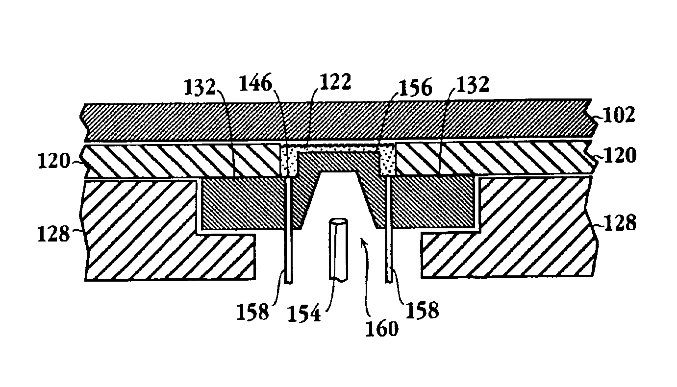
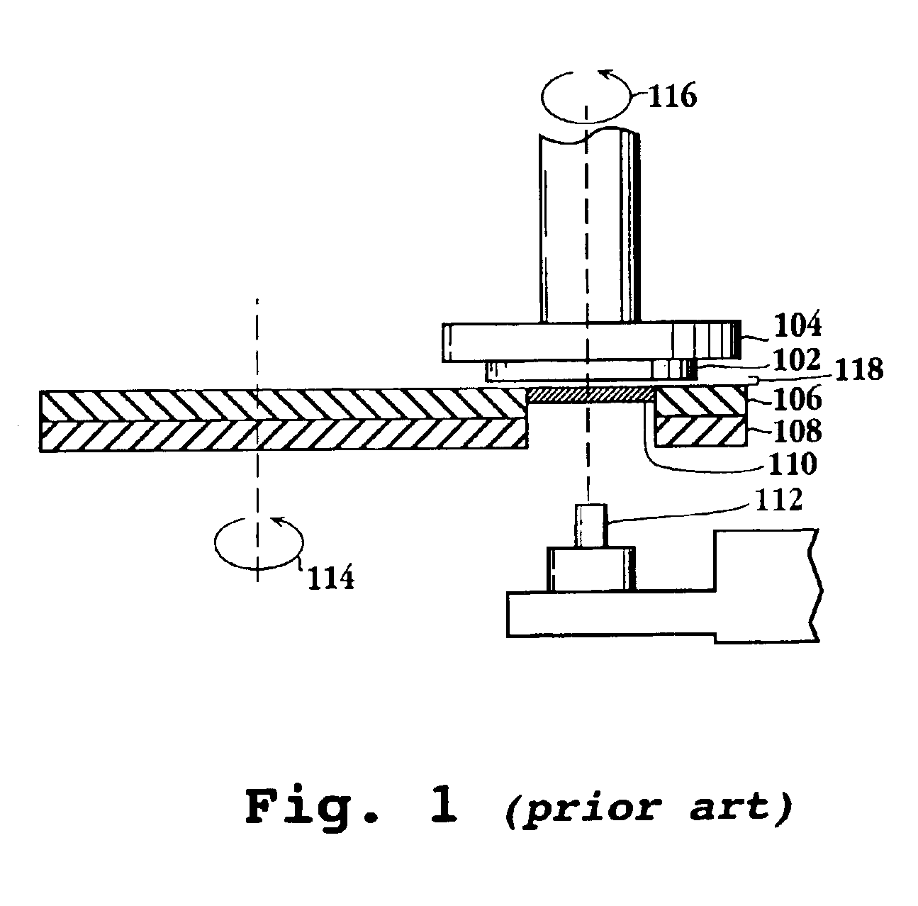
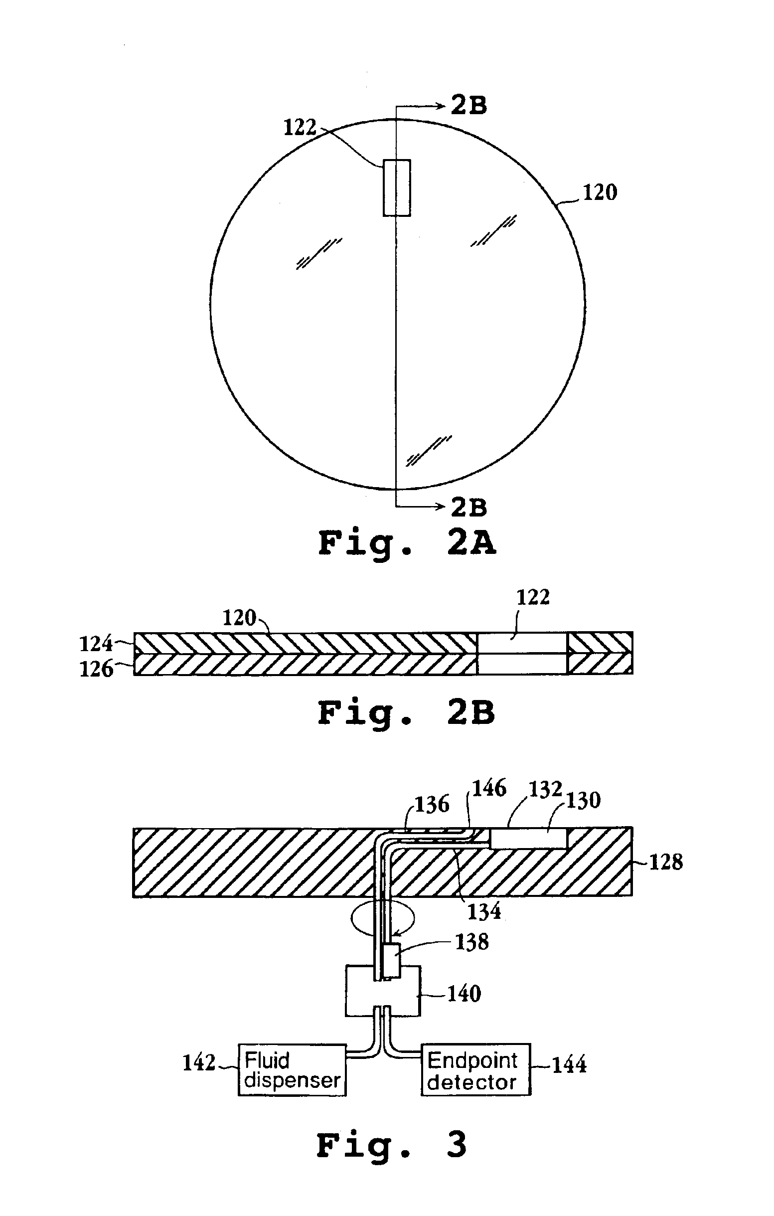
[0028]An invention is described for a method and apparatus which provides a substantially constant environment to accurately measure the thickness of a layer of a wafer during a chemical mechanical planarization (CMP) operation. It will be obvious, however, to one skilled in the art, that the present invention may be practiced without some or all of these specific details. In other instances, well known process operations have not been described in detail in order not to obscure the present invention.

[0029]The embodiments of the present invention provide an apparatus and method for maintaining a substantially constant environment in a cavity where an optical pathway traverses. The substantially constant environment minimizes any interference with in-situ thickness measurements of a wafer undergoing CMP. Additionally, by providing the stable environment, the conditions under which the in-situ end point detector is initially calibrated remain substantially constant throughout the CMP ...


PUM

PropertyMeasurementUnit
widthaaaaaaaaaa
widthaaaaaaaaaa
lengthaaaaaaaaaa

Abstract

A method and apparatus for providing a substantially constant environment in the cavity surrounding the optical pathway during the chemical mechanical planarization (CMP) operation is provided. In one embodiment, a system for planarizing the surface of a substrate is provided. The system includes a platen configured to rotate about its center axis. The platen supports an optical view-port assembly for assisting in determining a thickness of a layer of the substrate. A polishing pad disposed over the platen is included. The polishing pad has an aperture overlying a window of the optical view-port assembly. A carrier for holding the substrate over the polishing pad is also included. A cavity defined between the surface of the substrate and the window is included. A fluid delivery system adapted to provide a stable environment in the cavity during a chemical mechanical planarization (CMP) operation is included.

Description

CROSS REFERENCE TO RELATED APPLICATION[0001]This application is a continuation application of U.S. patent application Ser. No. 10 / 016,883, filed on Dec. 12, 2001 now U.S. Pat. No. 6,599,765, and entitled “APPARATUS AND METHOD FOR PROVIDING A SIGNAL PORT IN A POLISHING PAD FOR OPTICAL ENDPOINT DETECTION.” The disclosure of this related application is incorporated herein by reference for all purposes.BACKGROUND OF THE INVENTION[0002]1. Field of the Invention[0003]The invention relates generally to semiconductor manufacturing and more specifically to a method and apparatus for providing a stable environment for a signal transmitted to assist in determining the thickness of a layer of a semiconductor substrate.[0004]2. Description of the Related Art[0005]During semiconductor manufacturing, the integrated circuits defined on semiconductor wafers are manufactured by forming various layers over one another. As a result of the various layers disposed over one another a surface topography of...

Claims


Application Information

Patent Timeline
Patent Type & Authority Patents(United States)
IPC IPC(8): B24B37/04B24B49/12B24D13/00B24D13/14B24B37/20
CPCB24B37/205B24B49/12
Inventor BOYD, JOHN M.LACY, MICHAEL S.
Owner APPLIED MATERIALS INC
Why Eureka
Try Eureka