Method and apparatus for inspecting multilayer masks for defects

a multi-layer mask and mask technology, applied in the field of multi-layer mask inspection, can solve the problems of increasing the power needed, affecting the inspection effect, so as to achieve the effect of compact apparatus

Inactive Publication Date: 2005-10-11
NAT INST OF ADVANCED IND SCI & TECH
View PDF27 Cites 33 Cited by
  • Summary
  • Abstract
  • Description
  • Claims
  • Application Information

AI Technical Summary

Benefits of technology

[0027]By using a Schwarzschild optical system that enables a sufficient large magnification, an image detector having a large plurality of pixels and a plasma light source, the present invention makes it possible to detect small defects that are difficult to dete

Problems solved by technology

However, the fact that the patterns to be inspected are becoming smaller, and that there is not much difference between the reflectance of the substrate Mo/Si multilayer and that of the absorbing material that is to be inspected for pattern defects, makes it difficult to inspect reflective masks for defects by a visible layer.
Decreasing the is amount of tune allocated to exposure to reduce the time required for processing the data, results in an increase in the power that is needed.
How much power is actually required is something that has to be determined through future empirical investigation, but it is feared that more than a watt of power will be required.
However, because light cannot be focused to below its diffraction limit, the wavelength of the illuminating laser beam has to be shortened in order to decrease the size of the beam, meaning the size of the pixel.
However, it is not easy to decrease the laser wavelength to below 200 nm.
Because it is so difficult to achieve continuous laser oscillation at or belo

Method used


Image

  • Method and apparatus for inspecting multilayer masks for defects
  • Method and apparatus for inspecting multilayer masks for defects
  • Method and apparatus for inspecting multilayer masks for defects

Examples


Embodiment Construction

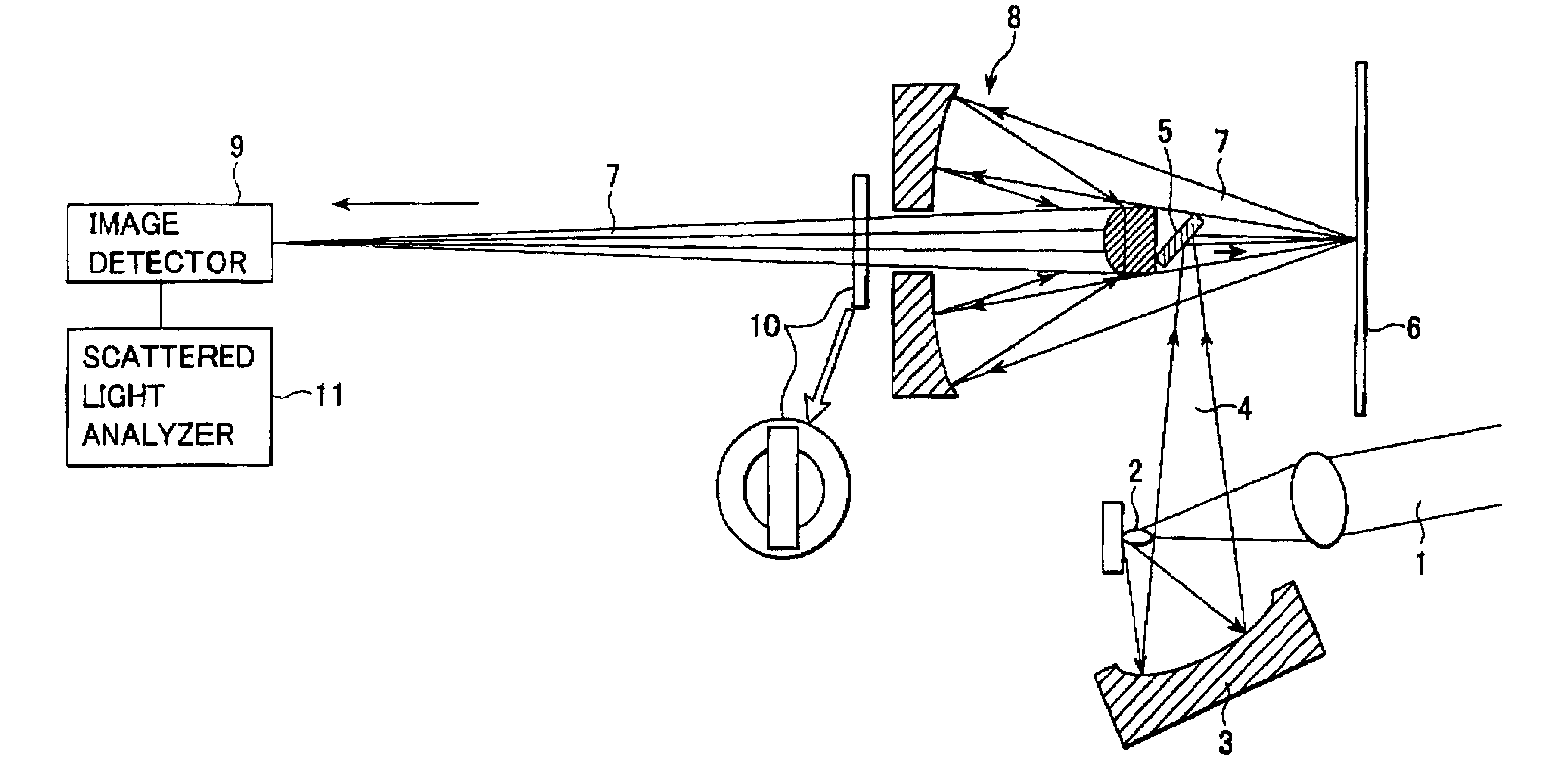
[0031]The present invention was perfected, as described below, after carrying out various considerations on inspection of defects on a multiplayer mask.

[0032]Specifically, as described above, dark-field observation makes it possible to detect defect-based signals with a very high contrast ratio, so that, as is clear from equation (1), it is possible to detect small defects within a large pixel. For the dark-field observation, it is necessary to use a light source having a wavelength that is near the peak of reflection spectrum of the multilayer reflective mask. As mentioned in the foregoing, Yi et al. demonstrated that it was possible to detect small defects within a large pixel in the dark-field observation with a synchrotron light source. However, the speed of the inspection by the method of Yi et al. was in the order of 1,000 times slower that what is needed in practice. Analyses carried out by the present inventors showed the reasons for this, which reasons are explained below.

[...


PUM


Abstract

A method for inspecting multilayer masks to detect any defects includes illuminating a pixel region on a mask to be inspected, using illuminating light having a peak wavelength that is close to that of light reflected by the mask. The illuminating light specularly reflected by the mask is blocked. Scattered reflected illuminating light is collected and used to form an enlarged image. An image detector having a large plurality of pixels is used to observe the enlarged image to detect whether there are defects on the mask. The method is implemented using an mask inspection apparatus including a plasma light source for generating radiant rays, an illuminating light collecting optical system that collects radiated light from the light source for enlarged image formation illumination of a subject inspection region, a Schwarzschild optical system including convex and concave mirrors for collecting scattered light from the subject inspection region and forming an enlarged image of the inspection region, an image detector having a large plurality of pixels for recording the enlarged image that is obtained, and an analyzer that analyzes the images obtained to determine whether there is a defect.

Description

BACKGROUND OF THE INVENTION[0001]1. Field of the Invention[0002]The present invention relates to a method for inspecting lithography multilayer masks for small defects, and to a defect inspection apparatus using the method.[0003]2. Description of the Prior Art[0004]Extreme ultraviolet (EUV) lithography (EUVL), in which an EUV light of 13 nm wavelength is employed as an illumination light, is the most promising lithography candidate for fabricating integrated circuits with a feature size of 70 nm or below. As such, related technologies are being developed.[0005]One such technology that needs to be developed is that of inspection of defects on a mask. Since all materials absorb EUV light strongly, EUVL utilizes a reflection mask. To obtain high reflectance for EUV light, a multilayer structure consisting of several tens of pairs of layers of Si and Mo, each approximately 3-nm thick, are formed by vapor deposition on an optical device surface. An EUVL mask is a reflective mask on top o...

Claims


Application Information

Patent Timeline
IPC IPC(8): G01N21/88G01N21/956G03F1/24G03F1/84G03F1/86H01L21/027
CPCG01N21/95623G03F1/24G03F1/84G01N21/33G01N2021/8822G01N2021/95676
Inventor TOMIE, TOSHIHISA
Owner NAT INST OF ADVANCED IND SCI & TECH
Why Eureka
Try Eureka