Stress-relief layer for semiconductor applications

a stress-relief layer and semiconductor technology, applied in semiconductor devices, semiconductor/solid-state device details, electrical apparatus, etc., can solve problems such as cracks in “hard” dielectrics, increased rc signal delay, and increased resistan

Inactive Publication Date: 2005-11-01
UNITED MICROELECTRONICS CORP +1
View PDF1 Cites 4 Cited by
  • Summary
  • Abstract
  • Description
  • Claims
  • Application Information

AI Technical Summary

Benefits of technology

[0011]The present invention can reduce the thermo-mechanical stress on vias and reduce cracking in the hard dielectric. Exemplary embodiments of the present invention can provide this by introducing a stress-relief layer between the vias and the hard dielectric layer. Such a stress-relief layer can include a “soft” dielectric material, such as a low-k insulating material.

Problems solved by technology

One result is an increase in RC signal delay.
In Cu / low-k interconnect architectures, the connecting vias between metal layers are subject to significant mechanical stresses that can result in, for example, via resistance increases.
Under stress, cracks can form in the “hard” dielectric.
These cracks can open the dielectric to environmental contamination, such as oxygen and moisture diffusion.

Method used


Image

  • Stress-relief layer for semiconductor applications
  • Stress-relief layer for semiconductor applications
  • Stress-relief layer for semiconductor applications

Examples


Embodiment Construction

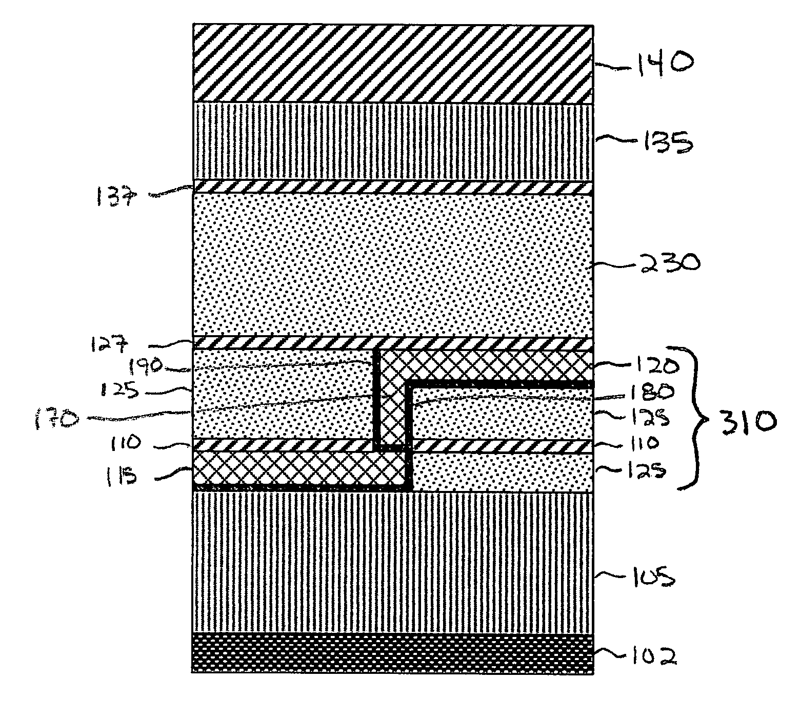
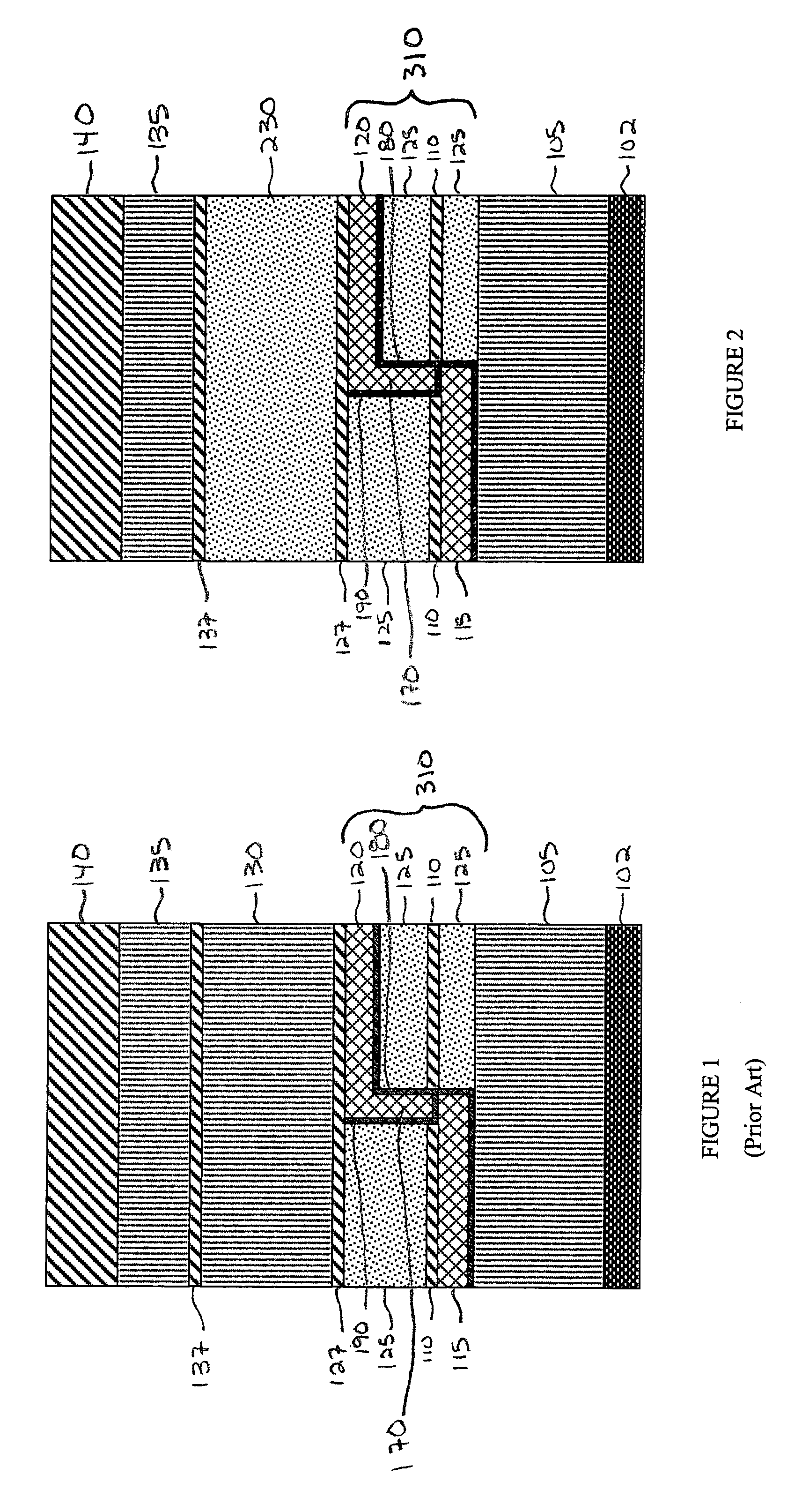
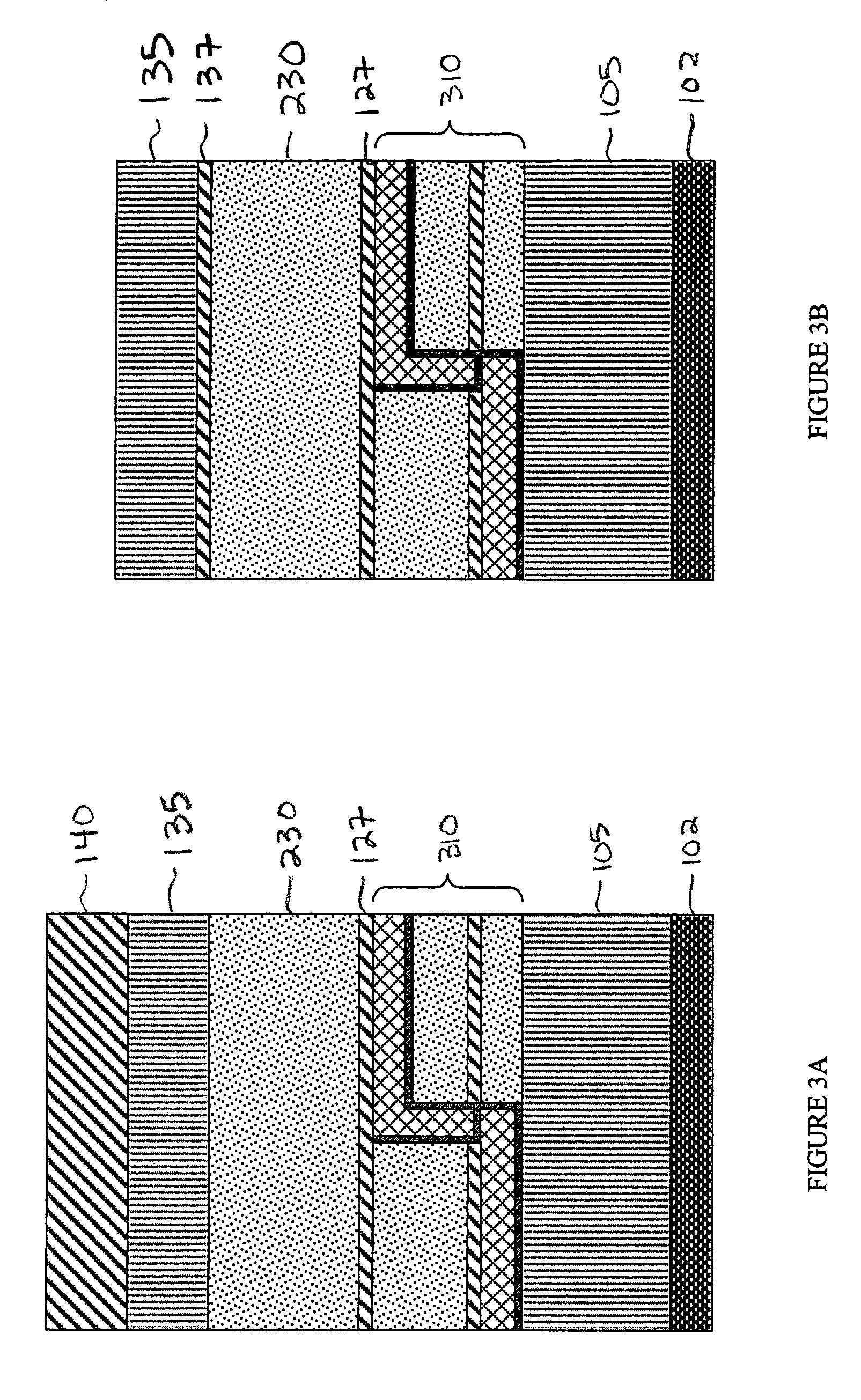
[0010]While the making and using of various embodiments of the present invention are discussed herein in terms of silicon low-k (“SiLK”) dielectric material, it should be appreciated that the present invention provides many inventive concepts that can be embodied in a wide variety of contexts. The specific embodiments discussed herein are merely illustrative of specific ways to make and use the invention, and are not meant to limit the scope of the invention.

[0011]The present invention can reduce the thermo-mechanical stress on vias and reduce cracking in the hard dielectric. Exemplary embodiments of the present invention can provide this by introducing a stress-relief layer between the vias and the hard dielectric layer. Such a stress-relief layer can include a “soft” dielectric material, such as a low-k insulating material.

[0012]FIGS. 1–3D are provided for illustrative purposes, and the various features therein are not necessarily shown to scale.

[0013]FIG. 1 diagrammatically illus...


PUM


Abstract

In a semiconductor integrated circuit device, thermo-mechanical stresses on the vias can be reduced by introducing a stress relief layer between the vias and a hard dielectric layer that overlies the vias.

Description

FIELD OF THE INVENTION[0001]The invention relates generally to semiconductor manufacturing and, more particularly, to a stress-relief layer for semiconductor applications.BACKGROUND OF THE INVENTION[0002]As semiconductor wafers progress to higher density chips with shrinking geometries, the materials and processes used in wafer fabrication are changing. At the same time, some chips have literally tens of billions of electrical connections between the various metal layers and silicon devices. Electrical performance is improved though concurrent scaling of device features. An indicator of chip performance is the speed at which signals are transmitted. Decreased geometries translate into reduced interconnect linewidths which in turn lead to increased resistance (“R”). Furthermore, reduced spacing between conductor lines creates more parasitic line capacitance (“C”). One result is an increase in RC signal delay. The line capacitance is directly proportional to the k-value of the dielect...

Claims


Application Information

Patent Timeline
Patent Type & Authority Patents(United States)
IPC IPC(8): H01L23/48H01L21/4763H01L21/02H01L29/00H01L21/768H01L23/532
CPCH01L21/76801H01L21/76829H01L21/76835H01L23/5329H01L23/53295H01L2924/0002H01L2924/00
Inventor BARTH, HANS-JOACHIMKALTALIOGLU, ERDEMHOINKIS, MARK D.FRIESE, GERALD R.LEUNG, PAK
Owner UNITED MICROELECTRONICS CORP
Why Eureka
Try Eureka