Waveguide plate and process for its production and microtitre plate

Inactive Publication Date: 2005-11-01
ZEPTOSENS +1
View PDF17 Cites 61 Cited by
  • Summary
  • Abstract
  • Description
  • Claims
  • Application Information

AI Technical Summary

Benefits of technology

[0016]Additionally, a highly precise optical element is to be provided such as can be produced by the process according to the invention. In particular, the optical element can be formed as a waveguide plate or an evanescent field sensor plate or as a microtitre plate based on such a plate. In view of the narrow limits within which, even in long gratings, the coupling angle varies, it is possible to simultaneously illuminate and read out larger parts of the waveguide plate or evanescent field sensor plate or microtitre plate. Successive exposure of different parts of the waveguide plate or the evanescent field sen

Problems solved by technology

Greater lengths are possible but require very long processing times. In practice, gratings of more than 1 mm2 can hardly be produced with reasonable effort and good accuracy.
In particular, stitching errors during inscribing by means of electron beams cannot be avoided.
All plates described above are produced by processes with which no satisfactory uniformity of the coupling grating can be achieved, so that the coupli

Method used


Image

  • Waveguide plate and process for its production and microtitre plate
  • Waveguide plate and process for its production and microtitre plate
  • Waveguide plate and process for its production and microtitre plate

Examples


Example

EXAMPLE 1

Design of a Waveguide Plate According to the Invention and Arrangement of Sample Compartments to be Formed by the Combination with Said Waveguide Plate

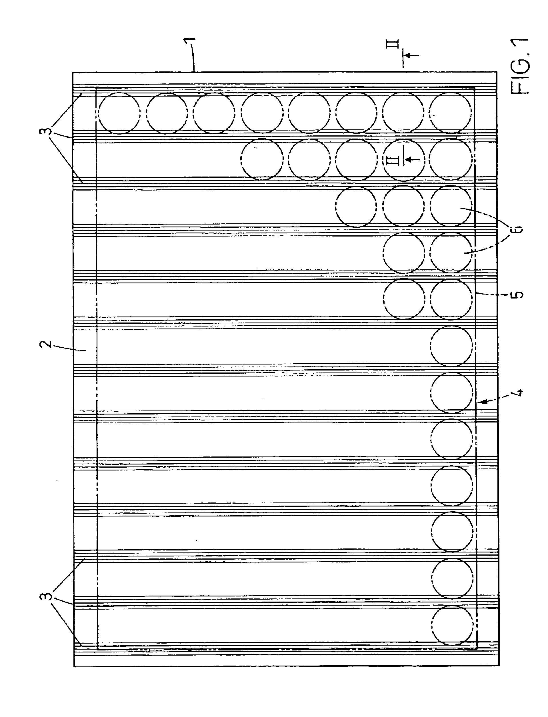
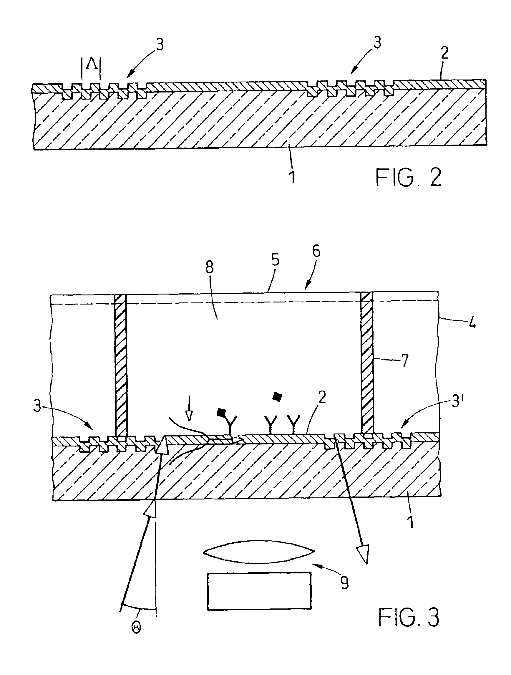
[0126]The waveguide plate according to the invention (FIGS. 1, 2 are schematically and not according to scale) comprises a glass substrate, for example of glass AF 45 from Schott DESAG, with dimensions of 102 mm×72 mm and a thickness of 0.7 mm, carrying on one surface a waveguiding layer 2 of Ta2O5 of 150 nm thickness. The refractive index is, dependent on the manufacturing method, for example 2.11 at 633 nm. Besides Ta2O5, also other materials are suited for the waveguiding layer, especially Nb2O5, TiO2, ZrO2, Al2O3, SiO2-TiO2, Hf02, Y2O3, SiOxNy, Si3N4, HfOxNy, AIOxNy, TiOxNy, MgF2 or CaF2.

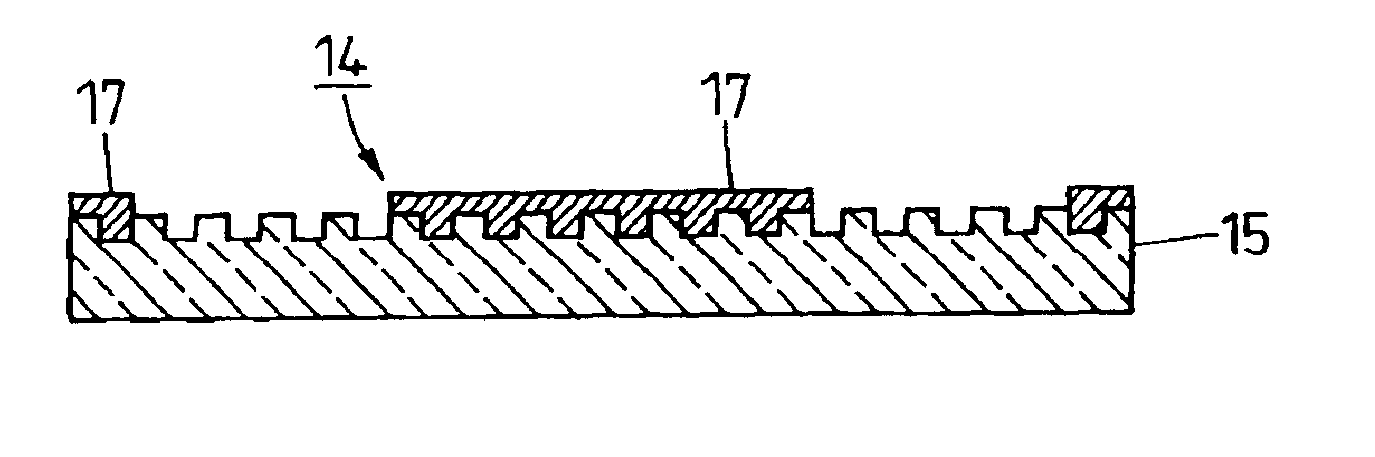
[0127]On the surface carrying the waveguiding layer 2, several coupling grating strips 3 are arranged in parallel to and separate from each other, extending in parallel lines over the whole width of the waveguide plate. The width of each ...

Example

EXAMPLE 2

Characterization of a Waveguide Plate According to the Invention

Example

[0130]A waveguide plate according to Example I (waveguiding layer of Ta2O5, refractive index n=2.11 at 633 nm ) is characterized. The waveguide plate is designed for use as a base plate for an arrangement of 96 sample compartments (provided as flowthrough cells) in a geometrical arrangement according to FIG. 1 (8 rows×12 columns of sample compartments). For the characterization of the physical properties of the waveguide plate, the following parameters shall be determined: (a) coupling angle and (b) the halfwidth of the resonance angle for maximum incoupling, (c) the lateral position (“x-position”) for optimum incoupling on a coupling grating strip and (d) its halfwidth, (e) the incoupling efficiency, (f) the number and size of scattering centers per area unit of the region of the sample compartments, analysis of (g) the excitation light profile for the region of the sample compartments, (h) background luminescence at the wavelength of the luminescence measurement for an analyte det...


PUM


Abstract

A waveguide plate and a process for making the waveguide plate with a plate-like glass substrate (1), carrying a waveguiding layer (2), with at least one coupling grating on the surface carrying said waveguiding layer (2), which coupling grating is formed as a grating of lines with a period between 150 nm and 1000 nm, the extension of said grating being at least 5 cm with lines parallel to one another, wherein the coupling angle () varies by not more than 0.1_/cm along a line of said grating and wherein the absolute value of the deviation of the coupling angle () on said waveguide plate, from a predefined desired value, does not exceed 0.5_. The deviation from the average value of the coupling angle does not exceed 0.3_, preferably not 0.15_ on the whole waveguide plate. The waveguide plate is suitable as part of a sensor platform and of an arrangement of sample compartments for chemo-and bioanalytical investigations in order to produce a coupling grating formed as a line grating with a grating period between 100 nm and 2500 nm

Description

CROSS-REFERENCE TO RELATED APPLICATIONS[0001]This application is a continuation-in-part of U.S. application Ser. No. 09 / 497,129 filed on Feb. 3, 2000 now U.S. Pat. No. 6,510,263.BACKGROUND OF THE INVENTION[0002]The invention relates to a waveguide plate and a process for its production and a microtitre plate comprising such a waveguide plate and as used, for example, for analytical purposes in the biochemical and medical sector, as well as a sensor platform based on a waveguide plate, an evanescent field sensor plate, according to the invention as well as arrangements of sample compartments, with a waveguide plate or a sensor platform according to the invention as a boundary surface of said arrangement of sample compartments. The invention also relates to an optical coupler and a device for monitoring such a coupler.[0003]The process according to the invention is suitable for producing optical elements with grating structures. Evanescent field sensor plates and microtitre plates pro...

Claims


Application Information

Patent Timeline
IPC IPC(8): G03F7/26G01N21/55G02B6/124G02B6/34G02B6/12G01N21/77
CPCG01N21/552G01N21/7743G02B6/124G02B6/136G02B6/34G02B2006/12107G02B2006/12147G01N21/648
Inventor MAISENHOELDER, BERNDEDLINGER, JOHANNESHEINE-KEMPKENS, CLAUSPAWLAK, MICHAELDUVENECK, GERT
Owner ZEPTOSENS
Why Eureka
Try Eureka