Device including a resistive path to introduce an equivalent RC circuit

a technology of resistive path and resistive circuit, which is applied in the direction of semiconductor devices, diodes, electrical apparatuses, etc., can solve the problems of standby power dissipation, power density and scalability, increase system performance, etc., and achieve the effect of raising the threshold voltage and lowering the threshold voltag

Inactive Publication Date: 2005-11-15
SUN MICROSYSTEMS INC
View PDF68 Cites 9 Cited by
  • Summary
  • Abstract
  • Description
  • Claims
  • Application Information

AI Technical Summary

Benefits of technology

[0043]In contrast to the structures and teachings of the prior art, the present invention includes a structure for providing at least one low power MOS device that includes a resistive well specifically designed to provide a resistive path between the bulk material of the device and a well tie contact. By providing a resistive path as taught by the invention, an equivalent RC circuit is introduced to the device that allows the bulk material potential to track the gate potential during switching, thereby lowering the threshold voltage as the device turns on and raising the threshold voltage as the device turns off. This gives devices designed according to the invention the positive attributes of prior art partially depleted SOI devices. However, the introduction of the resistive path, in accordance with the invention, also allows the bulk material potential to be controlled and stabilized at an equilibrium potential between clock periods. Therefore, devices designed according to the principles of the invention do not suffer from the floating body effect associated with prior art partially depleted SOI devices.

Problems solved by technology

In modern computer systems, power density and scalability issues represent some of the most significant obstacles to increased system performance.
However, lowering the threshold voltage of a device normally increases standby power dissipation by increasing device leakage and devices having low threshold voltages can leak so much current when their circuits are in a sleep or standby mode that the gains made by lowering the threshold voltage are outweighed by the power lost to leakage.
However, in the prior art, a significant amount of effort, and virtually all teaching, was directed to keeping V-bulk constant during a switching event and preventing significant changes in the potential of bulk material 106 during a switching event.
At these potentials, charge carriers acquire so much kinetic energy that the impact of the carriers at the drain end of the channel can result in the generation of electron-hole pairs.
In the prior art, if bulk material 106 were composed of even moderately resistive material, these sub-currents would result in large voltage drops throughout bulk material 106.
This short could draw enough current to not only shut down or “latch-up” the device, but in many cases, the current draw was large enough to physically destroy the device.
Therefore, while being very stable, prior art CMOS devices do not benefit from lower threshold voltages as the device turns on or relatively higher threshold voltages as the device turns off.
Consequently, prior art CMOS structures could not benefit from a variable V-bulk which tracks the gate potential and thereby lowers the threshold voltage as the device turns on.
As also discussed above, while prior art partially depleted SOI devices did allow the potential of the bulk material, V-bulk, to track the gate potential and thereby lower the threshold voltage as the device turned on, the floating body effect meant that the device typically did not return to an equilibrium potential between clock periods.

Method used


Image

  • Device including a resistive path to introduce an equivalent RC circuit
  • Device including a resistive path to introduce an equivalent RC circuit
  • Device including a resistive path to introduce an equivalent RC circuit

Examples


Embodiment Construction

[0091]The invention will now be described in reference to the accompanying drawings. The same reference numbers may be used throughout the drawings and the following description to refer to the same or like parts.

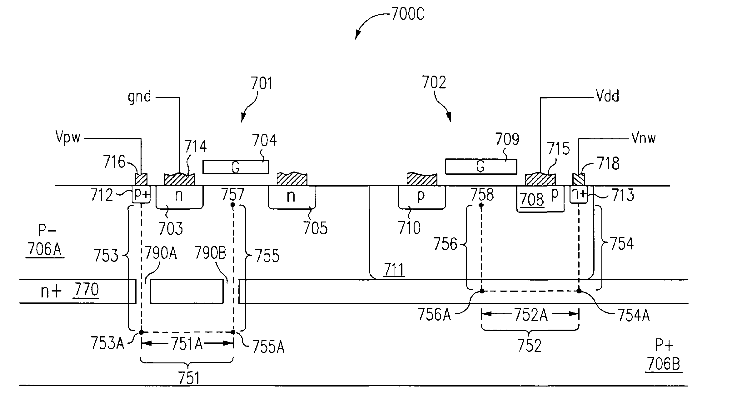
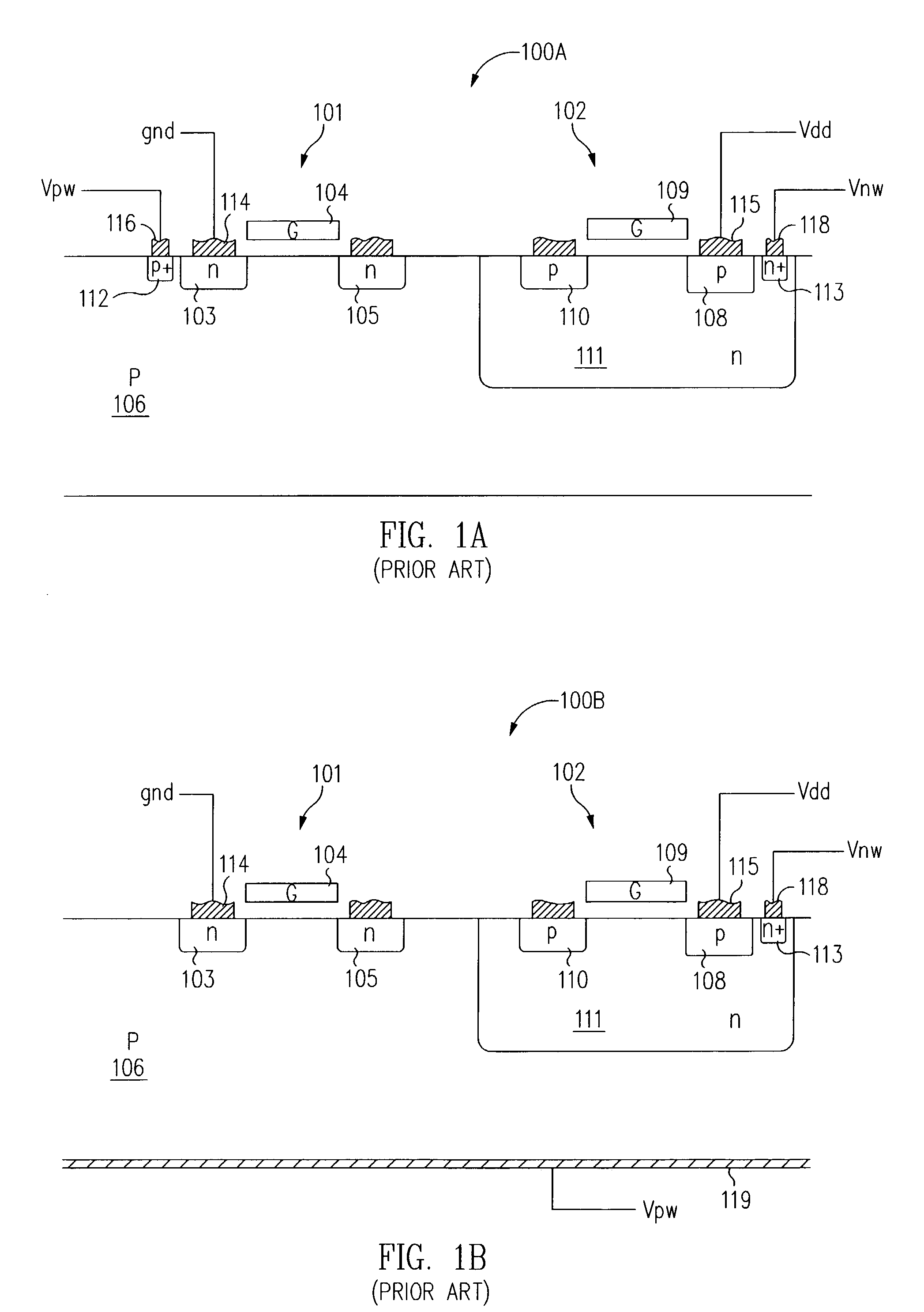
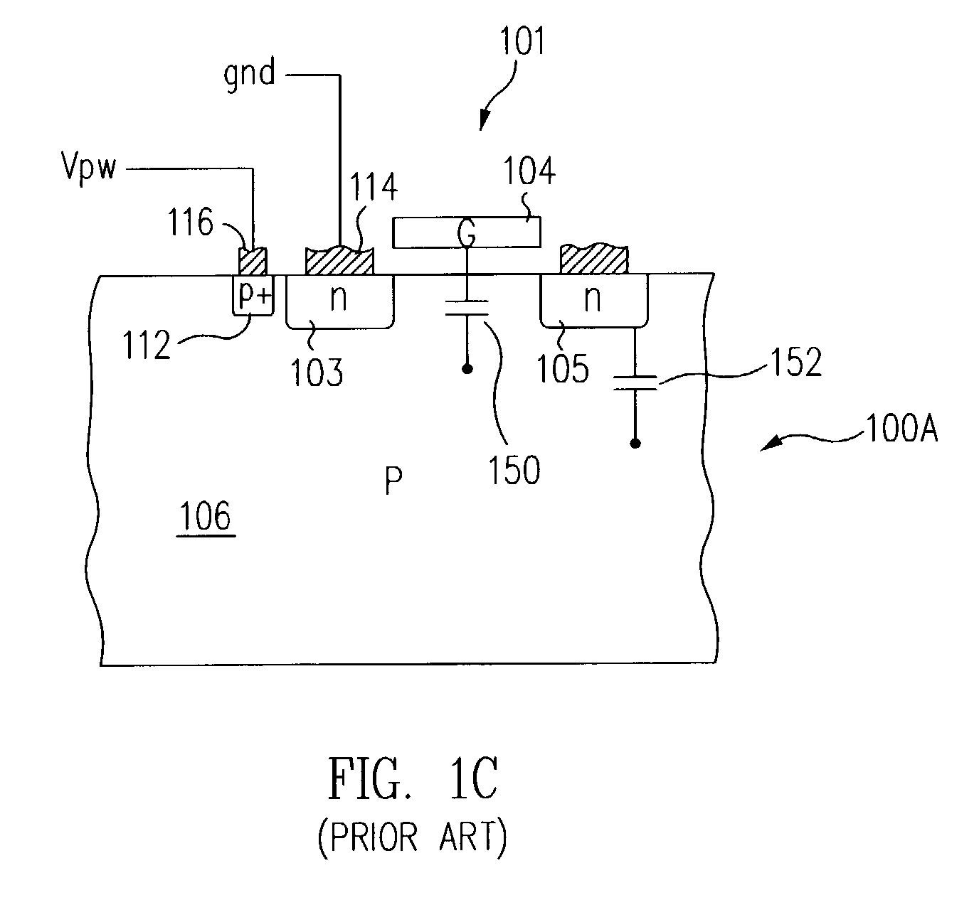
[0092]FIG. 3A illustrates a resistive well device 300A according to one embodiment of the invention. Device 300A includes an NFET 301 and a PFET 302 each of which is essentially a four-terminal device. NFET 301 is made up of an N-region source 303, a gate electrode 304, an N-region drain 305, formed in p-bulk material 306. Similarly, PFET 302 includes P-region source 308, a gate electrode 309 and a P-region drain 310 formed in an N-well bulk material 311. The device of FIG. 3A also includes a P plug that forms a well tie 312 and an N plug that forms a well tie 313.

[0093]In resistive well device 300A, according to one embodiment of the invention, well tie 312 is electrically isolated from source terminal 303 of the NFET 301 by providing a separate metallic rail contact 316 w...


PUM


Abstract

Structures for providing devices that include resistive paths specifically designed to provide a predetermined resistance between the bulk material of the device and a well tie contact. By providing a resistive path, an equivalent RC circuit is introduced to the device that allows the bulk material potential to track the gate potential, thereby advantageously lowering the threshold voltage as the device turns on and raising the threshold voltage as the device turns off. In addition, the introduction of the resistive path also allows the bulk material potential to be controlled and stabilize at an equilibrium potential between switching events.

Description

[0001]This application is a divisional of application Ser. No. 09 / 860,253, filed May 18, 2001, now U.S. Pat. No. 6,586,817.FIELD OF THE INVENTION[0002]The present invention relates generally to transistor devices and, more particularly, to low power and ultra-low power MOS devices.BACKGROUND OF THE INVENTION[0003]In modern computer systems, power density and scalability issues represent some of the most significant obstacles to increased system performance. For reliability, the supply voltage Vdd must come down and the threshold voltage must come up. Consequently, performance is being rapidly squeezed between the two. In addition, with the emergence of an electronics market that stresses portability, compact size, lightweight and the capability for prolonged remote operation, a demand has arisen for low power and ultra-low power transistor devices and systems. To meet this demand devices are emerging which have extremely low threshold voltages.[0004]There are a number of factors tha...

Claims


Application Information

Patent Timeline
Patent Type & Authority Patents(United States)
IPC IPC(8): H01L29/66H01L29/10H01L29/02H01L29/8605H01L27/085H01L27/07H01L27/092
CPCH01L27/0727H01L27/092H01L29/1087H01L29/8605
Inventor BURR, JAMES B.
Owner SUN MICROSYSTEMS INC
Why Eureka
Try Eureka