Method and apparatus for at-speed testing of digital circuits

a digital integrated circuit and self-testing technology, applied in error detection/correction, instruments, generating/distributing signals, etc., can solve problems such as increasing the number of devices within an ic for testing, increasing the difficulty of digital integrated circuit testing, and increasing the complexity of digital design

Inactive Publication Date: 2005-11-15
MENTOR GRAPHICS CORP
View PDF16 Cites 83 Cited by
  • Summary
  • Abstract
  • Description
  • Claims
  • Application Information

AI Technical Summary

Benefits of technology

[0019]Also disclosed is a method for testing a digital circuit that includes combinational logic interconnecting at least two interactive clock domains clocked at respective operating frequencies. The method includes providing a test pattern in the memory elements of a scan chain in the first clock domain. Each clock domain is then clocked at the domain's respective operating frequency, thereby launching the test pattern into the combinational logic. At a first time thereafter, a response to the test pattern is captured in the memory elements of a scan chain in one clock domain but not the other clock domain. This avoids the problems associated with clock skew when two clock domains attempt to simultaneously capture a test pattern response.

Problems solved by technology

The difficulty of testing digital integrated circuits is increasing at a rapid pace with the increasing complexity of digital design.
Access to devices within an IC for test, for example, has become a problem with the increase in device count.
The ratio of pin to device is gradually decreasing, resulting in increasing cost of test generation.
External testers are also becoming prohibitively expensive for testing multiple hundred Megahertz and Gigahertz frequency digital ICs.
Although BIST provides an alternative to external test, the issue of the quality of the testing remains the same for both paradigms.
Shrinking feature size together with multiple layers of metal connections in semiconductor processes is resulting into new failure modes.
AC failures are becoming equally important with static failures.
As clock speeds have reached Gigahertz frequencies, this had led to problems with the scan operation data in BIST.
First, shifting data through a scan chain results in simultaneous switching of large number of signals.
At high clock speeds, this shifting and switching generates very high power and heat that can damage the circuit under test.
Second, at-speed shifting often provides insufficient time for the scan enable control signal to change from a scan to capture state before the arrival of the capture edge of the clock.
In addition to problems with scan operations during at-speed testing, another challenge faced by BIST schemes is handling the multiple clock domains typically found in complex digital ICs.
Interaction of these clock-domains results in additional complexity in at-speed testing.
Both under-testing (testing at slower than the normal operating frequency) and over-testing (testing at faster than the normal operating frequency) can affect the quality and yield of the IC.
Method and apparatus for testing digital circuits with multiple clock domains are known, but each has significant drawbacks.
Moreover, inter-domain testing (where two clocks affect combinational logic through which the test data is propagated) is not done at speed, providing flawed results.
Another limitation of the described scheme is a limited ability to deal with clock skews (the inability to simultaneously clock a circuit with clocks from two domains).
Furthermore, inter-domain testing is not done at speed.
Moreover, the scan enable signal changes during the active edge of the clock, which may create a highly undesirable race condition.

Method used


Image

  • Method and apparatus for at-speed testing of digital circuits
  • Method and apparatus for at-speed testing of digital circuits
  • Method and apparatus for at-speed testing of digital circuits

Examples


Embodiment Construction

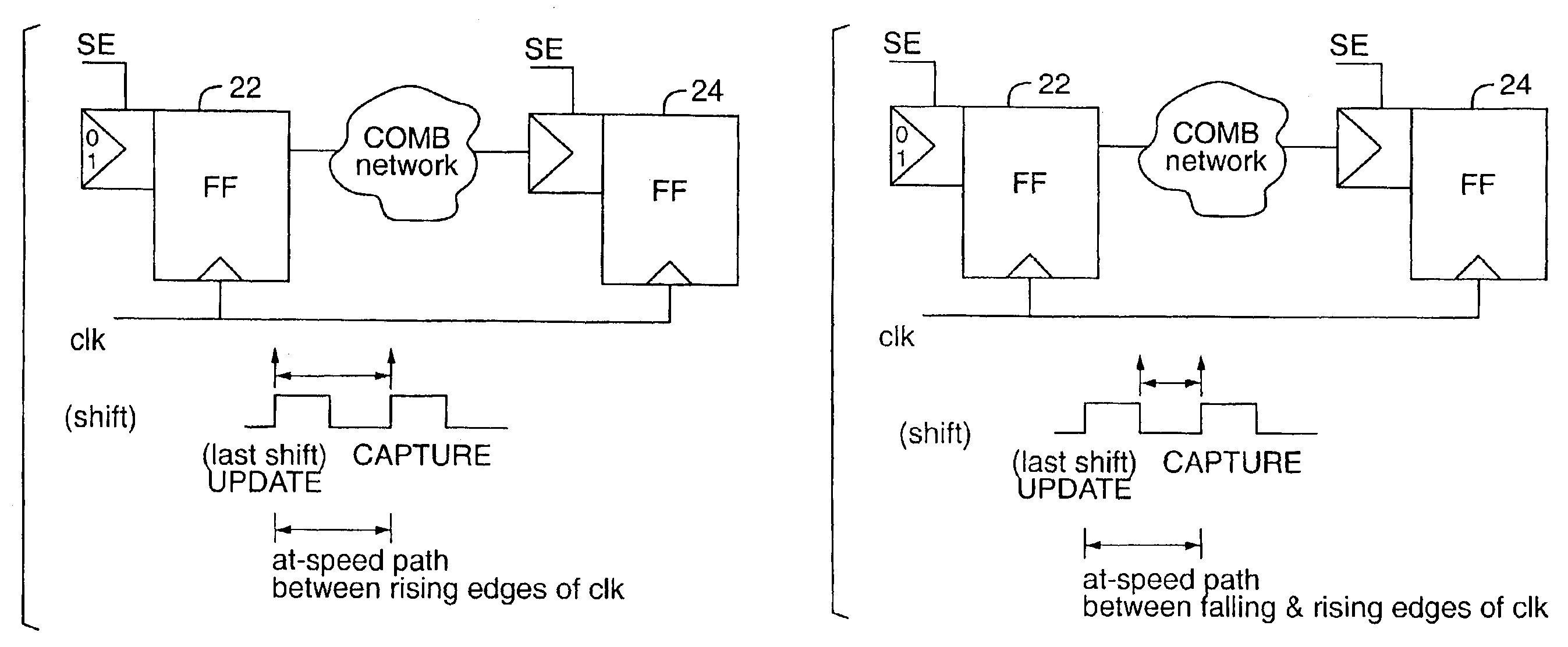
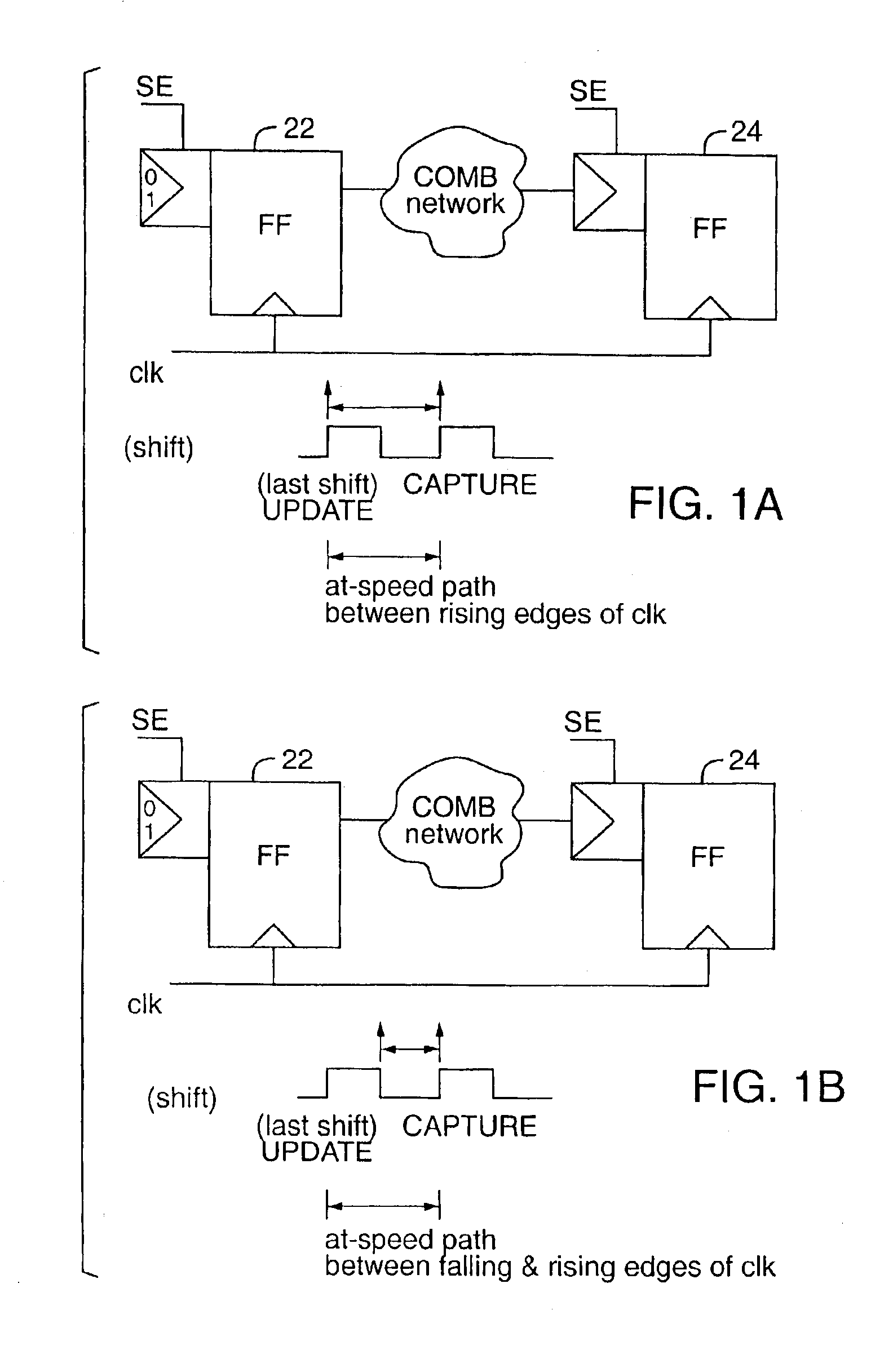
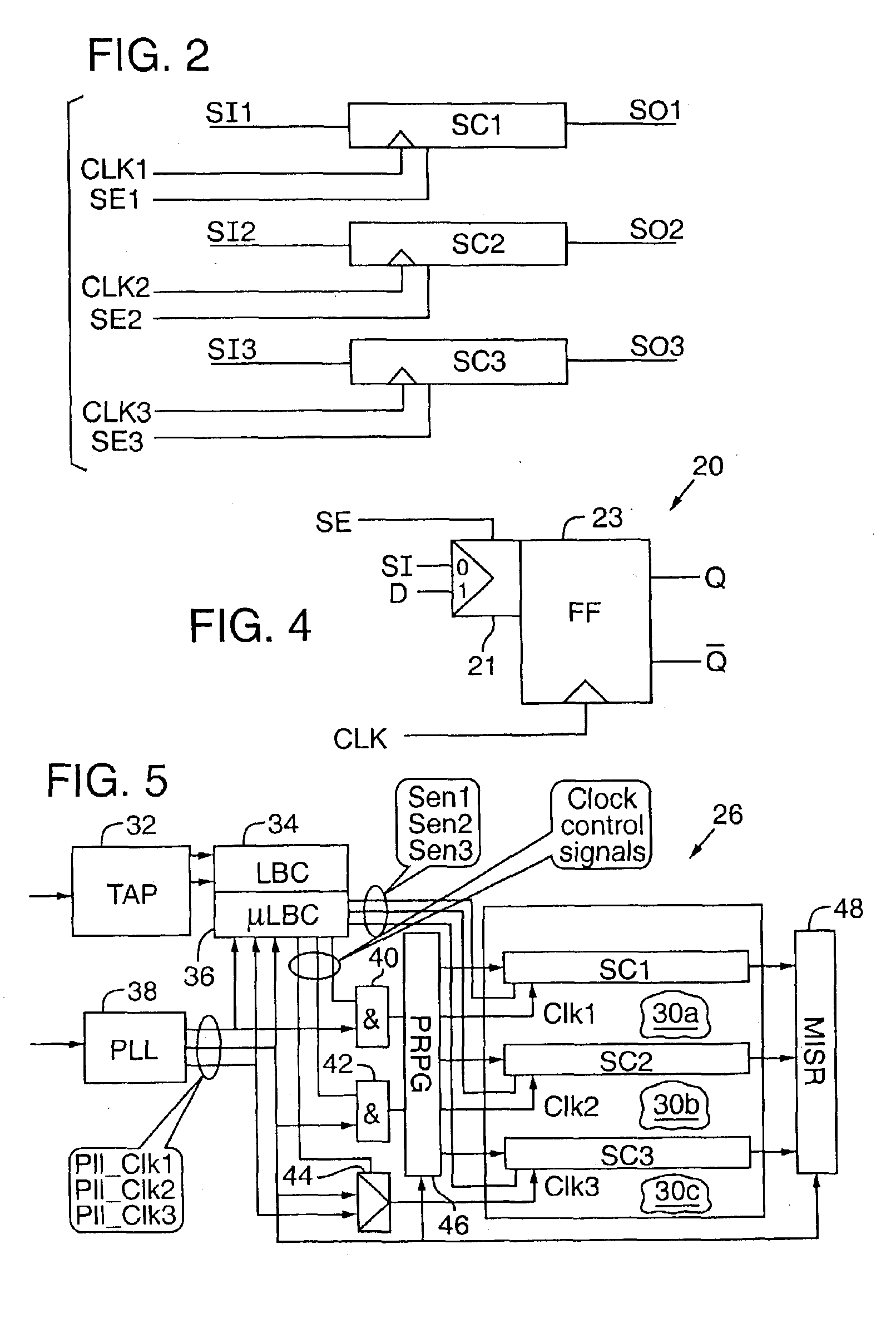
[0035]FIG. 4 is a block diagram of a memory element 20 such as a flip flop used as a sequential logic in a digital circuit and as a scan cell in a scan chain. The element includes a two-input multiplexer 21 coupled to the input of an edge-triggered flip flop 23. The two inputs to the multiplexer are data (D) and scan input (SI). The multiplexer control signal is called scan enable (SE) and it determines which of the multiplexer inputs are passed through to flip flop 23. The signal SE selects a test vector as input when the signal is in the scan state and selects data as input when the signal is in the capture state. The flip flop 23 (and hence memory element 20) is clocked by CLK. When the scan enable signal is in the scan state, CLK clocks a test pattern, or vector, sequentially via the SI input through the memory elements within the scan chain until the test vector is completely loaded therein. The combinational logic of the circuit design is decoupled from the scan chain during t...


PUM


Abstract

A scheme for multi-frequency at-speed logic Built-In Self Test (BIST) is provided. This scheme allows at-speed testing of very high frequency integrated circuits controlled by a clock signal generated externally or on-chip. The scheme is also applicable to testing of circuits with multiple clock domains which can be either the same frequency or different frequency. Scanable memory elements of the digital circuit are connected to define plurality of scan chains. The loading and unloading of scan chains is separated from the at-speed testing of the logic between the respective domains and may be done at a faster or slower frequency than the at-speed testing. The BIST controller, Pseudo-Random Pattern Generator (PRPG) and Multi-input Signature Register (MISR) work at slower frequency than the fastest clock domain. After loading of a new test pattern, a clock suppression circuit allows a scan enable signal to propagate for more that one clock cycle before multiple capture clock is applied. This feature relaxes the speed and skew constraints on scan enable signal design. Only the capture cycle is performed at the corresponding system timing. A programmable capture window makes it possible to test every intra- and inter-domain at-speed without the negative impact of clock skew between clock domains.

Description

RELATED APPLICATION DATA[0001]This patent is a continuation of U.S. patent application Ser. No. 09 / 342,162, filed Jun. 16, 1999, now abandoned which claims priority to U.S. Provisional Patent Application No. 60 / 089,620, filed Jun. 16, 1998, both of which are incorporated by reference herein.FIELD OF INVENTION[0002]This invention relates generally to the built-in self testing of integrated circuits (ICs). More specifically, the invention relates to at-speed self-testing of digital circuits that may have multiple clock domains.BACKGROUND OF THE INVENTION[0003]The difficulty of testing digital integrated circuits is increasing at a rapid pace with the increasing complexity of digital design. This testing typically occurs at the time of a circuit's manufacture, at start-up of a system that includes a circuit, or periodically while the circuit is functioning. With the technology delving into deep sub-micron feature size, digital designs are placing multi-million transistors in a single i...

Claims


Application Information

Patent Timeline
Patent Type & Authority Patents(United States)
IPC IPC(8): G01R31/28H02H3/05G01R31/3185
CPCG01R31/31858G01R31/318594
Inventor RAJSKI, JANUSZHASSAN, ABUTHOMPSON, ROBERTTAMARAPALLI, NAGESH
Owner MENTOR GRAPHICS CORP
Why Eureka
Try Eureka