Structure and method for fine pitch flip chip substrate
a technology of flip chip and substrate, which is applied in the direction of printing circuit manufacturing, printed circuit aspects, and metal adhesion improvement of the insulation substrate, etc., can solve the problems of poor adhesion of metal wires to the underfill and reduce reliability
- Summary
- Abstract
- Description
- Claims
- Application Information
AI Technical Summary
Benefits of technology
Problems solved by technology
Method used
Image
Examples
Embodiment Construction
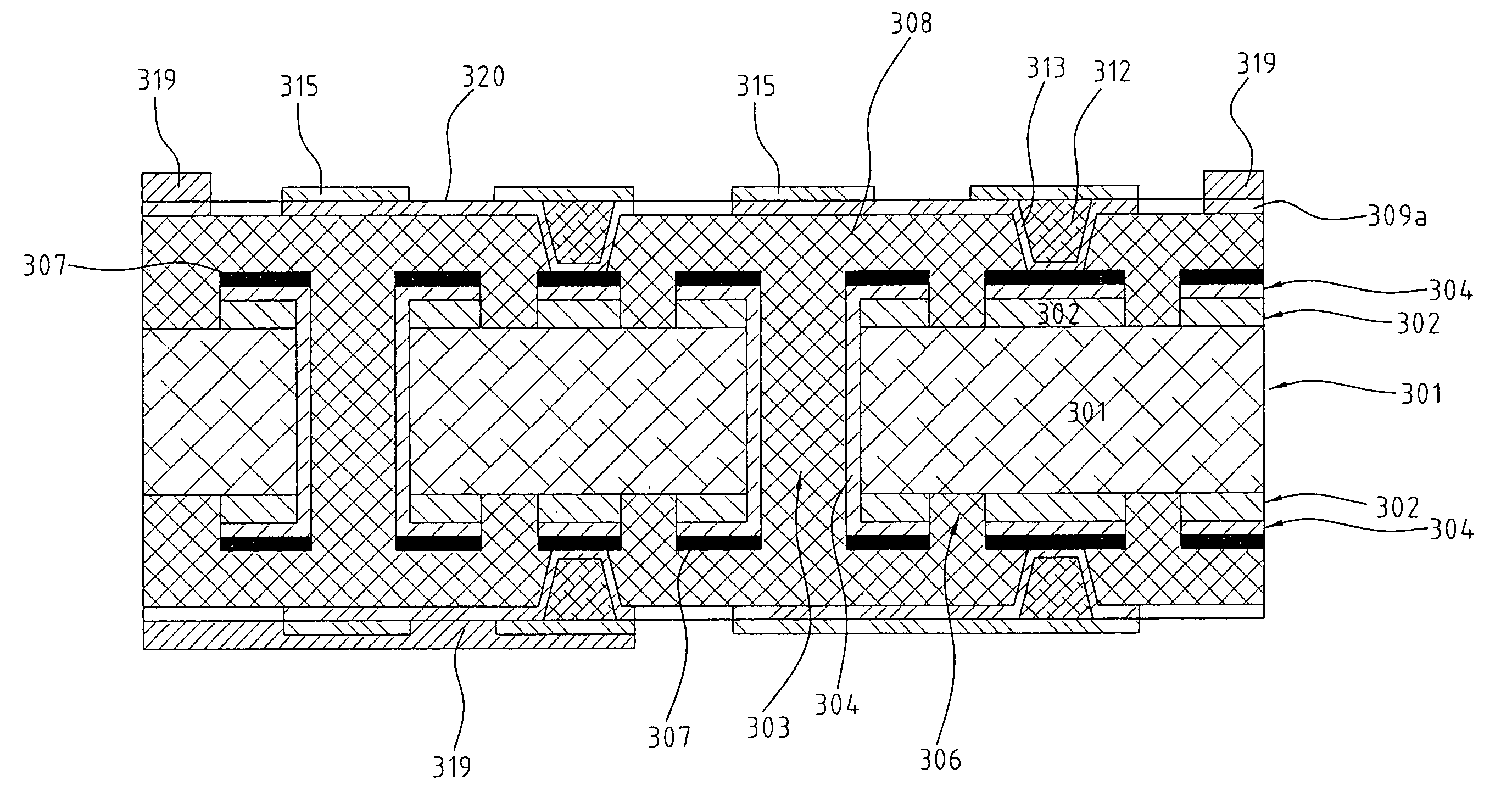
[0034]FIGS. 2A to 2T show the steps of the method for making a flip chip substrate including the following steps:
[0035]FIGS. 2A to 2C show a process of providing a substrate. FIG. 2A shows a substrate 201 which may be a flip chip substrate and is made of Bismaleimide Triazine (BT), other organic material, or even ceramics. The thickness of 201 is about 0.1 to 0.4 mm. A first metal layer 202 is made on the substrate 201. The first metal layer can be made of Copper (Cu) with a thickness of 12 μm. FIG. 2B shows a plurality of through holes 203 are drilled on the substrate 201 by mechanical or laser drilling. Each of the through holes 203 has a diameter of 100 to 250 μm. FIG. 2C shows that a first metal plated layer 204 is formed on the first metal layer 202 and the through holes 203. The first metal plated layer 204 can be made of Copper (Cu) with a thickness of 15 μm.
[0036]FIGS. 2D to 2E show a step of forming an inner circuit. FIG. 2D uses a dry film 205 containing an image to be tra...
PUM
 Abstract
Description
Claims
Application Information


