Method of making a planarized semiconductor structure

a semiconductor structure and planarized technology, applied in semiconductor/solid-state device manufacturing, basic electric elements, electric instruments, etc., can solve the problem of not forming a planar surface, reduce the use of polish stop layers, reduce step height, and reduce the effect of step coverage problems and lithography problems

Inactive Publication Date: 2005-11-29
INFINEON TECH LLC
View PDF110 Cites 6 Cited by
  • Summary
  • Abstract
  • Description
  • Claims
  • Application Information

AI Technical Summary

Benefits of technology

[0024]There may be several advantages to eliminating the use of a polish stop layer, and in some embodiments replacing it with a step-definition layer. For example, a shallow trench isolation region having a reduced step height may be formed. Such a benefit offers the formation of a substantially planar upper surface upon a semiconductor topography. In this manner, additional structures and layers may be formed within design specifications of the device. Furthermore, step coverage problems and lithography problems may be minimized. The method as described herein may also minimize pattern density constraints since the “dishing effect” is reduced. Other benefits may include a decrease in material use with a reduction in thickness of the upper layer and the elimination of the polish stop layer. Furthermore, the number of processing steps may be reduced. Such reductions and eliminations may reduce processing time, thereby increasing production throughput. Material costs and labor costs may also be reduced.

Problems solved by technology

In one embodiment, a substantially planar surface may not be formed upon termination of the polishing process if the thickness of overlying layers is not sufficient to form a substantially planar surface during the polishing process.

Method used


Image

  • Method of making a planarized semiconductor structure
  • Method of making a planarized semiconductor structure
  • Method of making a planarized semiconductor structure

Examples


Embodiment Construction

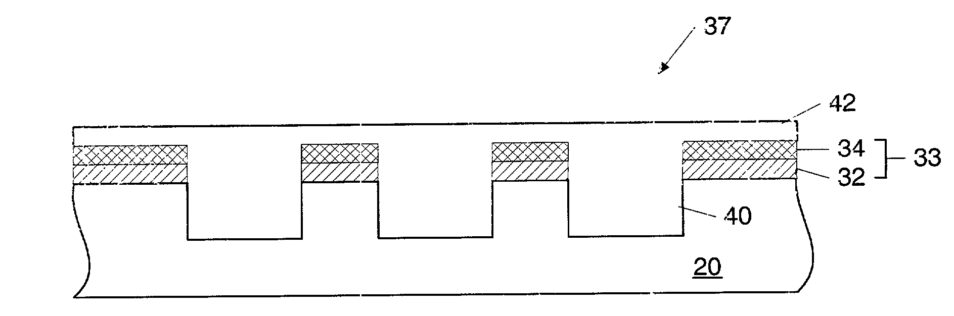
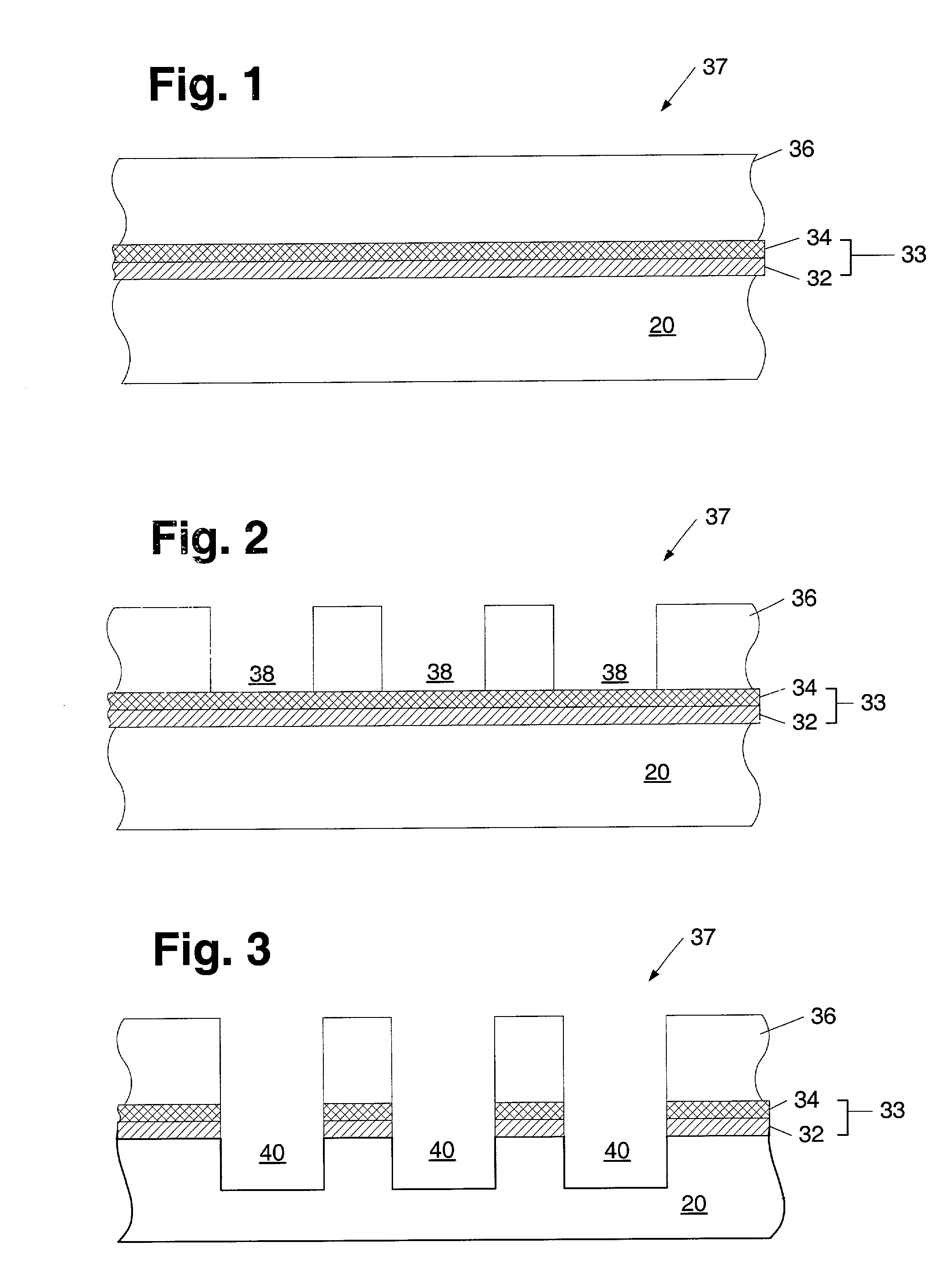
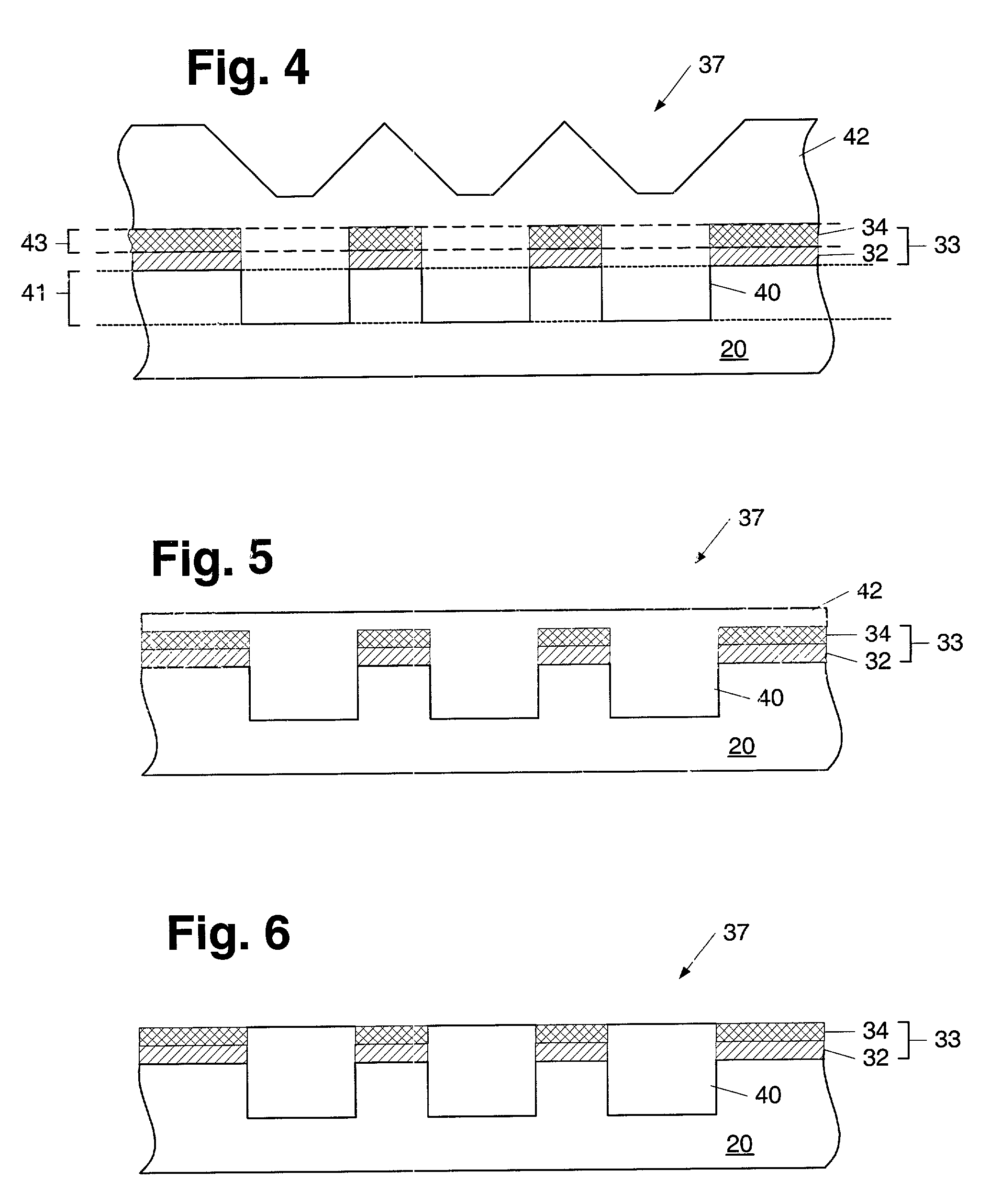
[0039]Turning to the drawings, exemplary embodiments of a method for processing a semiconductor topography are shown in FIGS. 1–12. In particular, a method is provided in which a polish stop layer may be eliminated from a polishing process. FIG. 1 depicts semiconductor topography 37 in which dielectric 32 may be formed upon semiconductor layer 20. Moreover, layer 34 may be formed upon dielectric 32, and resist 36 may be formed upon layer 34. Layers 32 and 34 may together form intermediate layer 33. Alternatively, intermediate layer 33 may include only either dielectric 32 or layer 34. In such an embodiment, the layer not included in intermediate layer 33 may be omitted. In particular, layer 34 may be omitted and thus resist layer 36 may be formed upon and in contact with underlying dielectric 32. Moreover, layer 34 may be formed upon and in contact with semiconductor layer 20 if dielectric 32 is omitted. In contrast, intermediate layer 33 may be omitted (omitting both layers 32 and ...


PUM


Abstract

A method is provided for eliminating a polish stop layer from a polishing process. In particular, a method is provided which may include polishing an upper layer of a semiconductor topography to form an upper surface at an elevation above an underlying layer, wherein the upper surface does not include a polish stop material. Preferably, the upper surface of the topography formed by polishing is spaced sufficiently above the underlying layer to avoid polishing the underlying layer. The entirety of the upper surface may be simultaneously etched to expose the underlying layer. In an embodiment, the underlying layer may comprise a lateral variation in polish characteristics. The method may include using fixed abrasive polishing of a dielectric layer for reducing a required thickness of an additional layer underlying the dielectric layer. Such a method may be useful when exposing an underlying layer is desirable by techniques other than polishing.

Description

BACKGROUND OF THE INVENTION[0001]1. Field of the Invention[0002]This invention relates to semiconductor device manufacturing, and more particularly, to an improved method for processing a semiconductor topography.[0003]2. Description of the Related Art[0004]The following descriptions and examples are not admitted to be prior art by virtue of their inclusion within this section.[0005]Forming substantially planar surfaces during the processing of a semiconductor topography may involve numerous fabrication steps. For example, a layer may be formed across a previously patterned layer of a semiconductor topography using a process such as chemical vapor deposition (“CVD”). Elevational disparities of the deposited layer may be reduced by planarizing the layer using a process such as chemical mechanical polishing (“CMP”). Alternatively, an opening or a trench may be formed within a semiconductor topography and subsequently filled with a layer of trench fill material. In this manner, the lay...

Claims


Application Information

Patent Timeline
Patent Type & Authority Patents(United States)
IPC IPC(8): H01L21/302H01L21/3105H01L21/762
CPCH01L21/31053H01L21/31055H01L21/76224
Inventor GILBOA, YITZHAKKOUTNY, JR., WILLIAM W. C.HEDAYATI, STEVENRAMKUMAR, KRISHNASWAMY
Owner INFINEON TECH LLC
Why Eureka
Try Eureka