Surface acoustic wave device, method for manufacturing, and electronic circuit device

a surface acoustic wave and manufacturing technology, applied in the direction of cable/conductor manufacturing, impedence network, generator/motor, etc., can solve the problems of affecting the efficiency of the device, affecting the reliability of the device, so as to achieve the effect of reducing cost and improving reliability

Inactive Publication Date: 2005-11-29
SKYWORKS PANASONIC FILTER SOLUTIONS JAPAN
View PDF10 Cites 43 Cited by
  • Summary
  • Abstract
  • Description
  • Claims
  • Application Information

AI Technical Summary

Benefits of technology

[0021]The present invention addresses the above problems and aims to offer a structure that can implement a small-area and low-profile surface acoustic wave device, which device also implementing a reduced

Problems solved by technology

These have been material factors that hindered the device downsizing.
Furthermore, a parasitic inductance intrinsic to thin metal wire 45 may deteriorate the high frequency characteristic of the element.
This has blocked the cost cutting efforts substantially.
However, reduction in the thickness is limited by the existence of a wiring board 54.
However, there are still a number of problems left to be solved before it is actually applied to the surface acoustic wave device.
Furthermore, due to

Method used


Image

  • Surface acoustic wave device, method for manufacturing, and electronic circuit device
  • Surface acoustic wave device, method for manufacturing, and electronic circuit device
  • Surface acoustic wave device, method for manufacturing, and electronic circuit device

Examples


embodiment 1

(Embodiment 1)

[0048]A first example of surface acoustic wave device in accordance with a first exemplary embodiment of the present invention is described with reference to the drawings.

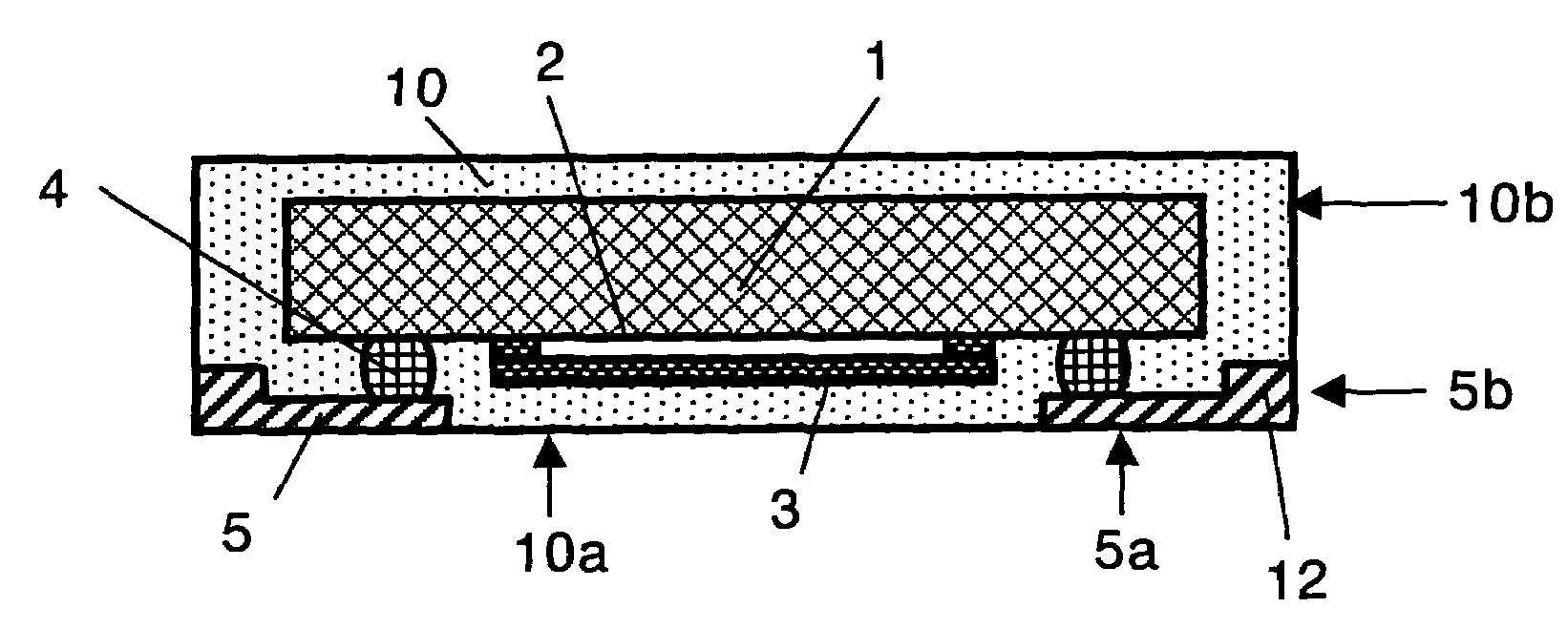
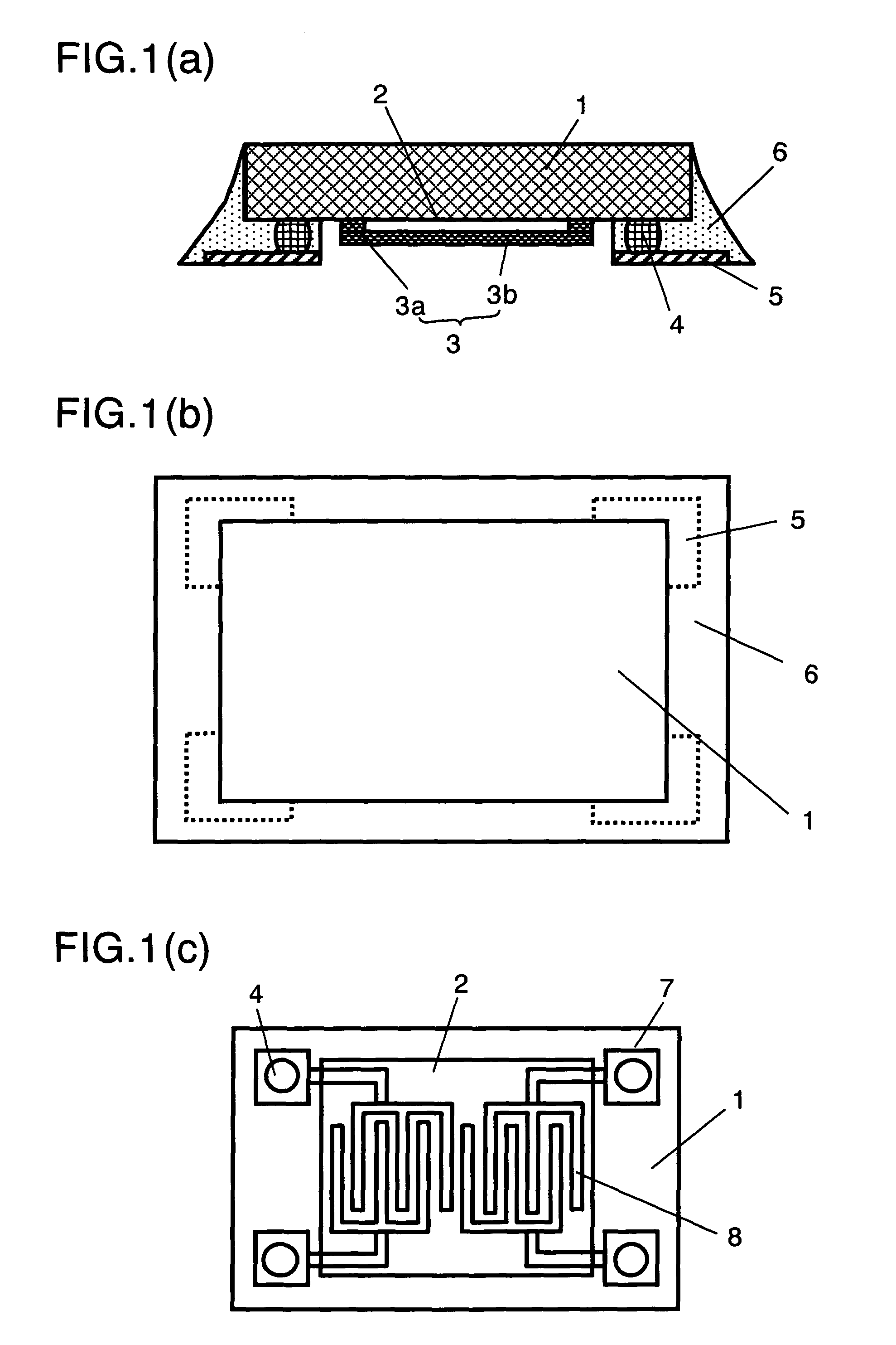
[0049]FIG. 1(a) is a cross sectional view used to describe a first example of surface acoustic wave device in accordance with a first exemplary embodiment of the present invention, FIG. 1(b) shows the device as viewed from the above, FIG. 1(c) is a drawing used to describe the surface acoustic wave element.

[0050]Size of a piezoelectric substrate 1 is 1.5×1.0 mm, and 0.3 mm thick. The terminology size used here means two-dimensional area of a device, and the same applies also to the other embodiments and examples. As to the material of the piezoelectric substrate 1, a single crystalline piezoelectric material such as lithium tantalate, lithium niobate, quartz, potassium niobate, langasite, etc. is used. Or a certain specific substrate provided with film of zinc oxide, aluminum nitride, etc. formed ther...

embodiment 2

(Embodiment 2)

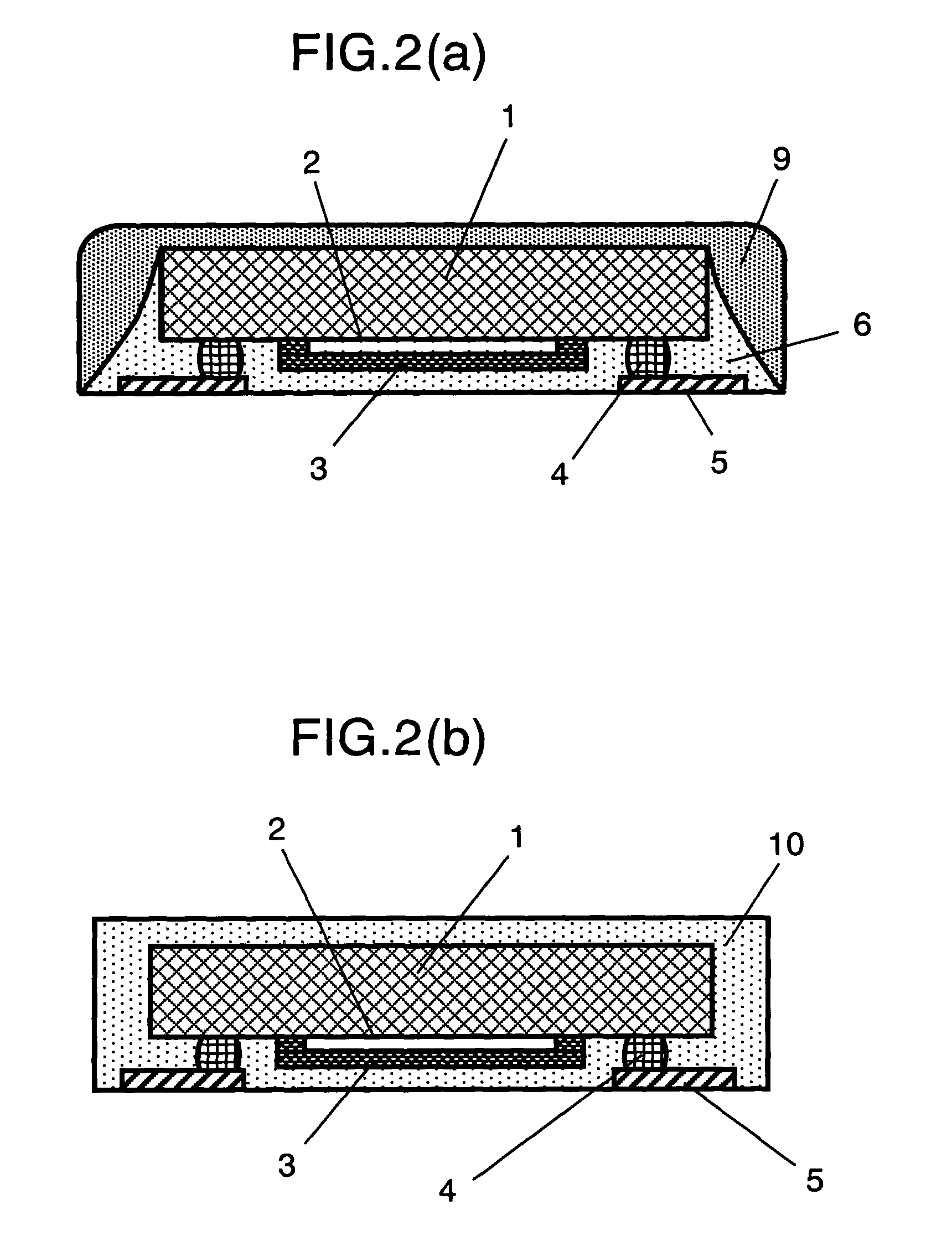
[0070]A first example of surface acoustic wave device in accordance with a second exemplary embodiment of the present invention is described referring to FIG. 5(a).

[0071]The first example shown in FIG. 5(a) uses a surface acoustic wave element, which comprises a piezoelectric substrate 1 provided with a function region 2, a space formation member 3 covering the function region 2, and a bump electrode 4 provided on the main surface; the bump electrode 4 is electrically connected with the terminal electrode, and the entire structure is sealed with a sealing resin 10. In addition, a conductor island 13 is provided corresponding to the function region 2. Thus, a thin and compact surface acoustic wave device having the above-described structure where the surface acoustic wave element is built in and the function region 2 is protected with respect to electro-magnetic property and reliability by the conductor island 13 is implemented.

[0072]That it is “protected with respect t...

embodiment 3

(Embodiment 3)

[0078]A first example of method for manufacturing surface acoustic wave device in accordance with a third exemplary embodiment of the present invention is described referring to the drawings.

[0079]FIG. 6(a) through (c) are cross sectional views showing the process steps used to describe a first example of manufacturing method of surface acoustic wave device in accordance with the third embodiment of the present invention.

[0080]As shown in FIG. 6(a), a surface acoustic wave element is prepared, which element comprising a piezoelectric substrate 1 provided with a function region 2 having comb-like electrodes, etc., an electrode pad (not shown), and a bump electrode 4 formed on the surface, the function region 2 being covered with a space formation member 3.

[0081]The comb-like electrode and the electrode pad of surface acoustic wave element are formed by a sputtering process and a photolithography. The comb-like electrode is made with aluminum, or an aluminum alloy, e.g. ...


PUM

PropertyMeasurementUnit
Thicknessaaaaaaaaaa
Adhesivityaaaaaaaaaa

Abstract

A surface acoustic wave device which occupies a small mounting area and has a low profile, yet having an improved reliability, and can be made available at low cost. The surface acoustic wave device comprises a piezoelectric substrate, a function region formed of comb-like electrodes for exciting surface acoustic wave provided on a main surface of the piezoelectric substrate, a space formation member covering the function region, a plurality of bump electrodes provided on a main surface of the piezoelectric substrate and a terminal electrode provided opposed to the main surface of piezoelectric substrate. The bump electrode and the terminal electrode are having a direct electrical connection, and a space between piezoelectric substrate and terminal electrode is filled with resin. When the above-configured acoustic wave device is applied for a frequency filter, a resonator, in a portable telephone unit, a keyless entry or the like communication apparatus, the overall size of such apparatus can be reduced and a higher reliability is implemented.

Description

[0001]This application is a U.S. National Phase Application of PCT International Application PCT / JP02 / 00949.TECHNICAL FIELD[0002]The present invention relates to a surface acoustic wave device used as frequency filter or resonator in a portable telephone unit, a keyless entry and the like communication devices. It also relates to a high frequency module containing the surface acoustic wave device.BACKGROUND ART[0003]Portable telephone units and the like portable information terminal apparatus are making remarkable evolution towards the compactness in size, lightness in weight and slimness in overall contour. So, for the semiconductor devices and other electronic components such as filter, resonator, etc., it is an essential requirement to be consistent with the above trends if they are to be adopted in such recent apparatus.[0004]An example of such components is disclosed in Japanese Patent Laid-Open Application No. H10-270975; a surface acoustic wave device, in which the surface ac...

Claims


Application Information

Patent Timeline
IPC IPC(8): H01L21/68H03H3/08H03H9/05
CPCH01L21/568H01L24/97H03H3/08H03H9/0542H03H9/059H03H9/1085H03H9/1092H01L21/6835Y10T29/49144H01L2224/16H01L2224/48091H01L2224/48227H01L2224/97H01L2924/01003H01L2924/01013H01L2924/01029H01L2924/0103H01L2924/01033H01L2924/01039H01L2924/01046H01L2924/01047H01L2924/01057H01L2924/01058H01L2924/01078H01L2924/01079H01L2924/01082H01L2924/15153H01L2924/1517H01L2924/16195H01L2924/30105H01L2924/30107H01L2924/3025Y10T29/42Y10T29/49158Y10T29/49171Y10T29/49146Y10T29/49005H01L2924/01005H01L2924/01006H01L2924/01019H01L2924/01021H01L2924/01024H01L2224/45144H01L2224/81H01L2924/00014H01L2224/16245H01L2924/16235H01L2924/181H01L2924/351H01L2924/00H01L2924/00012
Inventor NAMBA, AKIHIKOONISHI, KEIJISUGAYA, YASUHIROMORITOKI, KATSUNORI
Owner SKYWORKS PANASONIC FILTER SOLUTIONS JAPAN
Why Eureka
Try Eureka