Apparatus for inspecting defects of devices and method of inspecting defects

a technology for inspecting devices and defects, applied in the direction of individual semiconductor device testing, contactless testing, instruments, etc., can solve the problems of poor accuracies of moving positions, inability to observe sim images of circuit wiring patterns of all tegs formed within one chip without moving the sample stage, etc., and achieve high reliability

Inactive Publication Date: 2005-11-29
HITACHI LTD +1
View PDF23 Cites 18 Cited by
  • Summary
  • Abstract
  • Description
  • Claims
  • Application Information

AI Technical Summary

Benefits of technology

[0011]According to the present invention, firstly, electric charges are supplied to a device (a semiconductor chip, for example) in such a manner that an electrically isolated component (wiring, for example) thereof has a different voltage from an electrically grounded component (a substrate, for example) thereof (Step 1). Next, voltage contrast data of the chip including the above-described components are obtained by use of an SIM image (Step 2). Lastly, any component showing a voltage different from a predetermined voltage with respect to such component is detected by analyzing the voltage contrast data (Step 3). In Step 1, supply of the electric charges occurs in the course of irradiating

Problems solved by technology

Nevertheless, even if coverage of the one TEG unit being the square of 1 to 2.5 mm is achieved, it is yet impossible to observe SIM images of circuit wiring patterns of all TEGs formed with

Method used


Image

  • Apparatus for inspecting defects of devices and method of inspecting defects
  • Apparatus for inspecting defects of devices and method of inspecting defects
  • Apparatus for inspecting defects of devices and method of inspecting defects

Examples


Embodiment Construction

[0043]Now, the present invention will be described in detail with reference to the accompanying drawings.

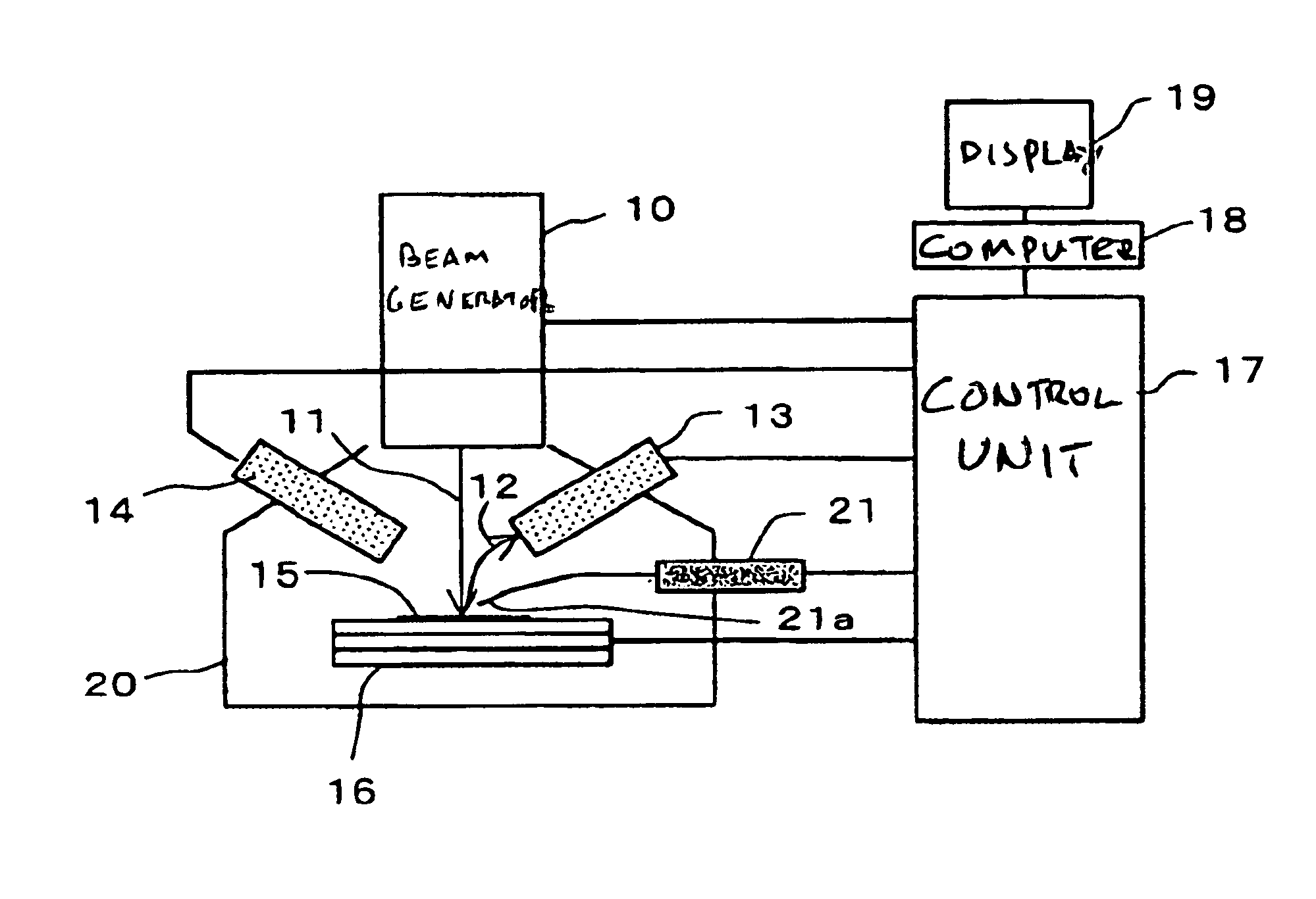
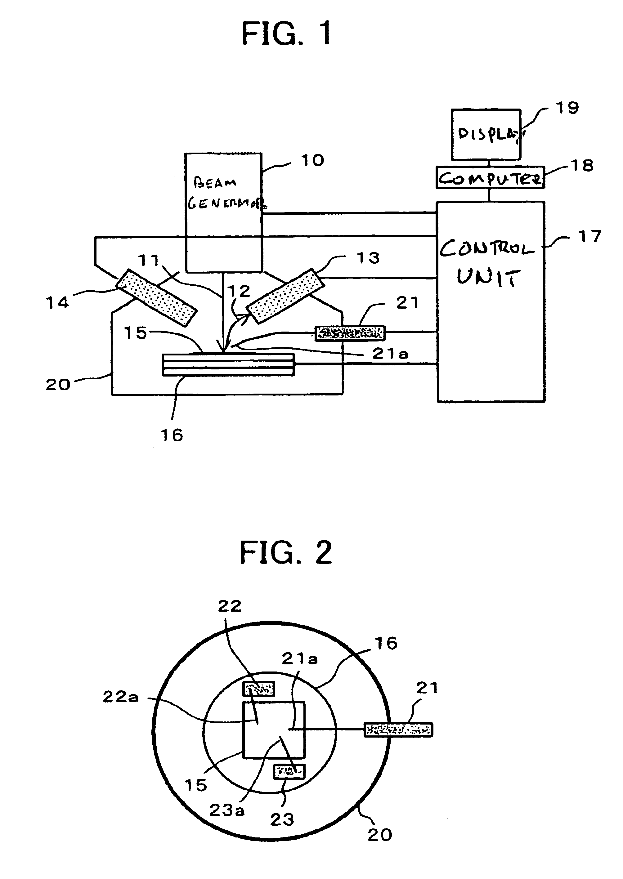
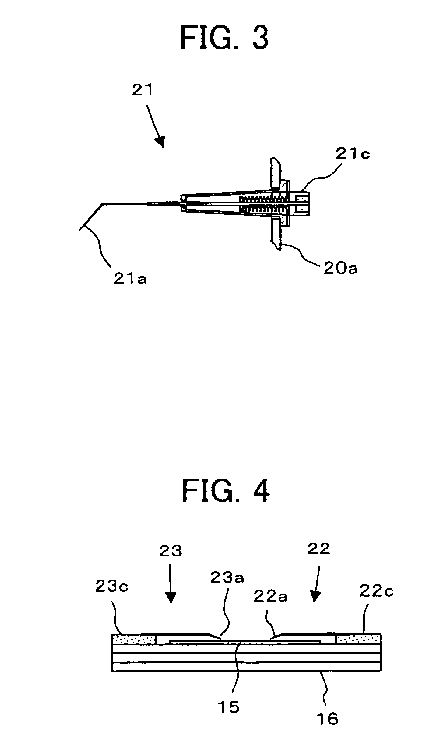
[0044]FIG. 1 is a schematic constitutional view of an apparatus for inspecting defects of devices according to the present invention, and FIG. 2 is a schematic top plan view of a sample 15, a sample stage 16 and conductor probe means 21, 22 and 23 inside a sample chamber of the apparatus for inspecting defects of devices shown in FIG. 1, viewed from a direction of an FIB axis. An FIB generator 10 generates an FIB 11 by drawing ions out of a gallium liquid metal ion source and focusing the ions by acceleration to 30 kV. An electric current of the FIB is in a range from about 1 pA to 20 nA. Normally, the electric current in a range from 1 pA to 100 pA is used for observation of an SIM image of defects; the electric current at several tens of picoamperes is used for conductive film deposition by the FIB assist; and the electric current in a range from several tens of picoamperes to ...


PUM


Abstract

Disconnection defects, short-circuit defects and the like in wiring patterns of submicron sizes within TEGs (a square of 1 to 2.5 mm for each) numerously arranged in a large chip (a square of 20 to 25 mm) can be inspected with respect to all the TEGs, with good operability, high reliability and high efficiency. A conductor probe for applying voltage to the wiring patterns by mechanical contact is composed of synchronous type conductor probe that synchronizes with movement of a sample stage (16), and fixed type conductor probe means (21) that is relatively fixed to an FIB generator (10). Positions of probe tips are superimposed to an SIM image and displayed on a display unit (19).

Description

[0001]This application is a continuation of application Ser. No. 09 / 936,941, filed Dec. 4, 2001 now U.S. Pat. No 6,734,687 is a 371, which in turn of PCT / JP00 / 01108, filed Feb. 25, 2000, the subject matter of both of which is incorporated by reference herein.BACKGROUND OF THE INVENTION[0002]1. Technical Field[0003]The present invention relates to an apparatus for inspecting defects of devices and a method of inspecting defects, in particular, to an apparatus for inspecting defects of devices useful for detecting defects of disconnection and short circuits of electric wiring and a method of inspecting defects.[0004]2. Description of the Prior Art[0005]A manufacturing process of a semiconductor is composed of iteration of serial processes such as exposure, etching, film forming and doping. Depending on maturity of a manufacturing process used, defect (form defects and electrical defects) inspection and dimension measurement are carried out between processes. From a viewpoint of early ...

Claims


Application Information

Patent Timeline
IPC IPC(8): G01R31/265G01R31/28G01R31/302G01R31/303G01R31/305G01R31/307G01R31/311H01J37/20H01J37/28
CPCG01R31/303G01R31/311G01R31/2851
Inventor ISHITANI, TOHRUKOIKE, HIDEMISUGIMOTO, ARITOSHISEKIHARA, ISAMUUMEMURA, KAORUTOMIMATSU, SATOSHIAZUMA, JUNZO
Owner HITACHI LTD
Why Eureka
Try Eureka