Thermosensitive flow rate detecting element and method for the manufacture thereof
a flow rate detection and flow rate technology, applied in the direction of filtration separation, instruments, separation processes, etc., can solve the problems of change in resistance in the joint portion, fluctuation of flow rate detection characteristics, and decrease of bonding strength between the conductor and the electrically-conductive film, etc., to achieve stable flow rate detection characteristics
- Summary
- Abstract
- Description
- Claims
- Application Information
AI Technical Summary
Benefits of technology
Problems solved by technology
Method used
Image
Examples
embodiment 1
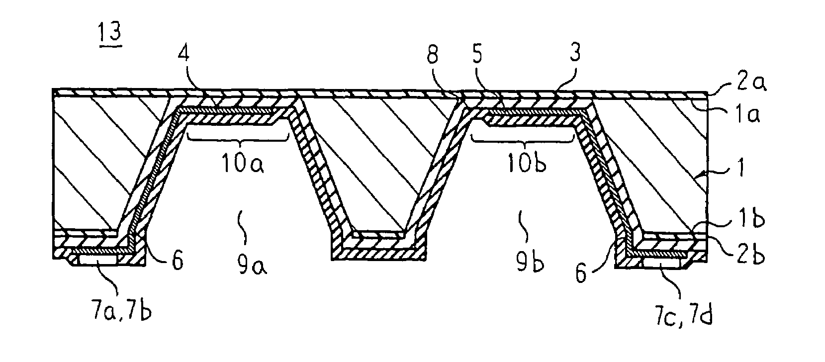
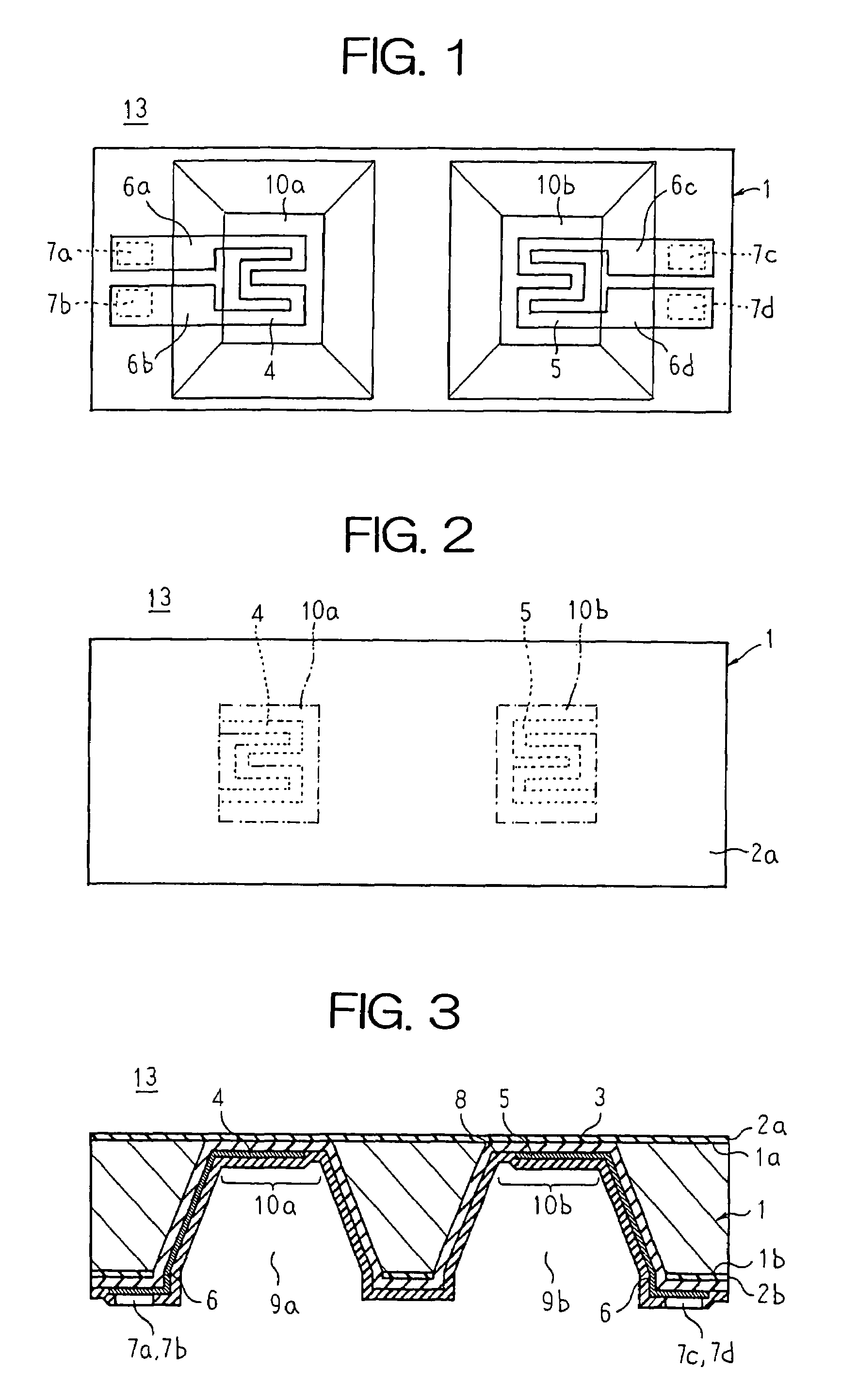
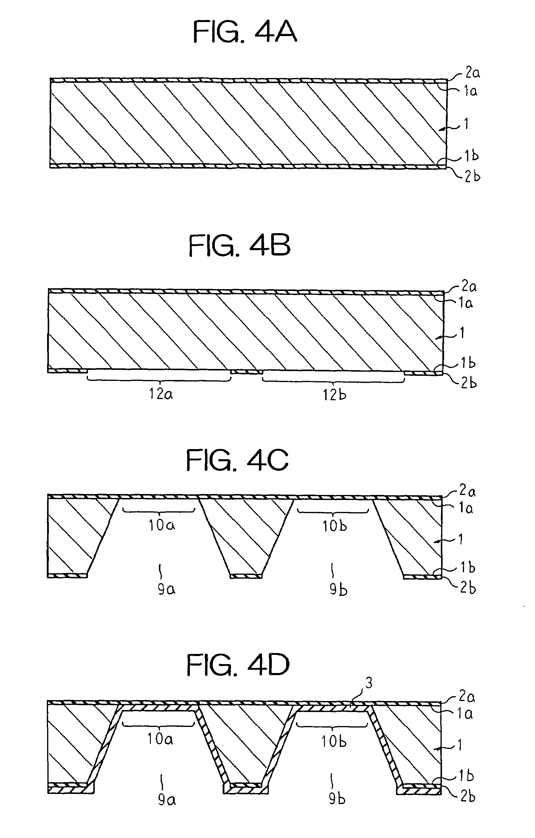
[0034]FIG. 1 is a bottom plan showing a thermosensitive flow rate detecting element according to Embodiment 1 of the present invention, FIG. 2 is a top plan showing the thermosensitive flow rate detecting element according to Embodiment 1 of the present invention, and FIG. 3 is a cross section showing the thermosensitive flow rate detecting element according to Embodiment 1 of the present invention. Moreover, a rear-surface protective film is omitted from FIG. 1. In order to make the construction easier to see, FIGS. 1 to 3 are not drawn to actual scale. This also applies to all of the figures below.
[0035]In FIGS. 1 to 3, a base material 1 is a silicon substrate formed into a flat, rectangular shape, for example. A first protective film 2a composed of a thermal oxidation film, etc., is formed over an entire surface of a front surface 1a of the base material 1. A second protective film 2b composed of a thermal oxidation film, etc., is formed over an entire surface of a rear surface 1...
embodiment 2
[0067]FIG. 9 is a cross section showing a thermosensitive flow rate detecting element according to Embodiment 2 of the present invention.
[0068]In FIG. 9, a base material 1A is an alumina substrate formed into a flat, rectangular shape, for example. An electrically-insulating film 3a composed of a silicon nitride film, etc., is formed over an entire surface of a front surface 1a of the base material 1A. A protective film 3b composed of a silicon nitride film, etc., is formed over an entire surface of a rear surface 1b of the base material 1A so as to have two rectangular aperture portions. First and second cavities 9a and 9b are formed by removing portions of the base material 1A so as to extend to the electrically-insulating film 3a from each of the aperture portions of the protective film 3b.
[0069]A heating resistor portion 4 composed of a thermosensitive resistor film of platinum, etc., is formed on an exposed surface of the electrically-insulating film 3a inside the first cavity...
PUM
| Property | Measurement | Unit |
|---|---|---|
| thickness | aaaaa | aaaaa |
| thickness | aaaaa | aaaaa |
| thickness | aaaaa | aaaaa |
Abstract
Description
Claims
Application Information


