Semiconductor package with enhanced electrical and thermal performance and method for fabricating the same

a technology of semiconductor chips and electrical and thermal performance, which is applied in the direction of semiconductor devices, semiconductor/solid-state device details, electrical apparatus, etc., can solve the problems of unsuitable packaging unsatisfactory heat dissipation efficiency of packaged semiconductor chips, and unsuitable use of semiconductor chips having a large number of power and ground pads, etc., to achieve good emi shielding effect, improve electrical performance during operation

Inactive Publication Date: 2005-12-06
SILICONWARE PRECISION IND CO LTD
View PDF2 Cites 11 Cited by
  • Summary
  • Abstract
  • Description
  • Claims
  • Application Information

AI Technical Summary

Benefits of technology

[0015]An objective of this invention is to provide a semiconductor package with enhanced electrical and thermal performance, which provides good EMI (electromagnetic interference) shielding effect.
[0016]Another objective of this invention is to provide a semiconductor package with enhanced electrical and thermal performance, by which satisfactory heat-dissipation efficiency is achieved.
[0017]A further objective of this invention is to provide a semiconductor package with enhanced electrical and thermal performance, wherein the semiconductor package is cost-effectively fabricated.
[0020]The above package structure is characterized by the use of a specially-designed set of power-connecting heat spreader and ground-connecting heat spreader, which are each electrically connected to and structured to entirely cover an underlying chip. Thereby, the power-connecting heat spreader allows external power to be efficiently supplied to the chip, and the ground-connecting heat spreader would provide good EMI shielding effect for allowing the chip to improve its electrical performance during operation. Further, a top surface of the ground-connecting heat spreader is adapted to be exposed to outside of an encapsulation body that encapsulates the chip, thereby helping enhancing heat-dissipation efficiency for the package structure.

Problems solved by technology

One drawback to this patent, however, is that it is unsuitably used for packaging semiconductor chips having a great number of power and ground pads.
One drawback to the forgoing BGA package, however, is that, since the ground-connecting heat spreader 130 only covers part of the semiconductor chip 110, it would not be able to provide good EMI (electromagnetic interference) shielding effect for the semiconductor chip 110 during operation.
Moreover, since both the power-connecting heat spreader 120 and the ground-connecting heat spreader 130 are completely enclosed by the encapsulation body 150, they may not provide satisfactory heat-dissipation efficiency for the packaged semiconductor chip 110.

Method used


Image

  • Semiconductor package with enhanced electrical and thermal performance and method for fabricating the same
  • Semiconductor package with enhanced electrical and thermal performance and method for fabricating the same
  • Semiconductor package with enhanced electrical and thermal performance and method for fabricating the same

Examples


Embodiment Construction

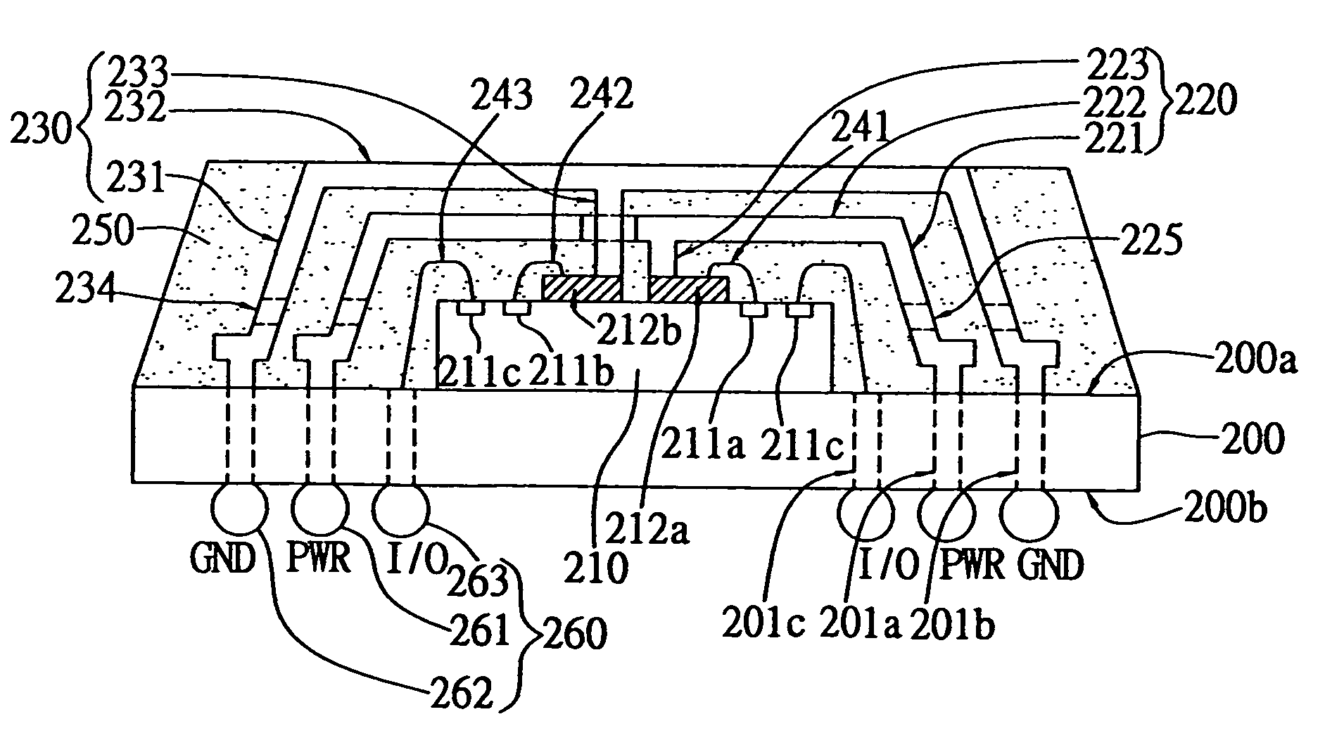
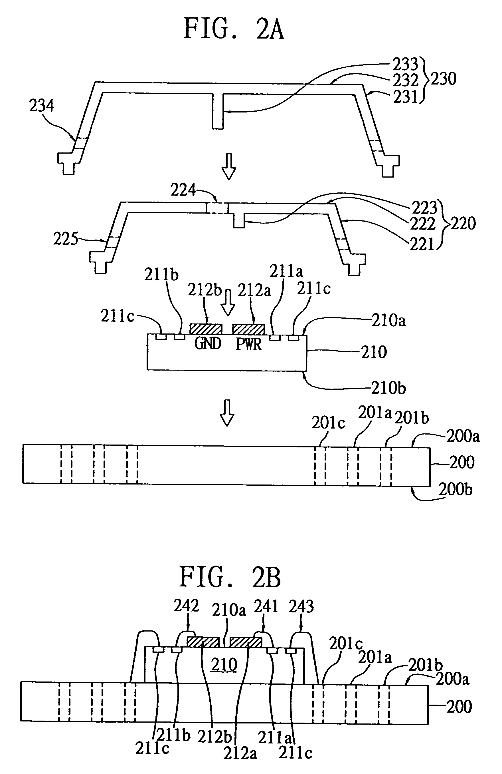
[0024]The following description is made with reference to FIGS. 2A–2E, for detailing preferred embodiments of a BGA (ball grid array) semiconductor package proposed in the present invention.

[0025]As shown in FIG. 2E, the BGA semiconductor package of the invention comprises: a substrate 200 having a front surface 200a and a back surface 200b opposed to the front surface 200a; at least a chip 210 having an active surface 210a and an inactive surface 210b opposed to the active surface 210a, wherein the active surface 210a is formed with a power plane 212a and a ground plane 212b, and the inactive surface 210b is mounted on the front surface 200a of the substrate 200; a power-connecting heat spreader 220 adapted to entirely cover the chip 210, and electrically bonded to the front surface 200a of the substrate 200 and the power plane 212a on the chip 210; a ground-connecting heat spreader 230 positioned in elevation above the power-connecting heat spreader 220, and adapted to be electric...


PUM


Abstract

A BGA (ball grid array) package with enhanced electrical and thermal performance, and a method for fabricating the BGA package, are proposed. This BGA package is characterized by the use of a power-connecting heat spreader and a ground-connecting heat spreader, which are respectively used to electrically connect power pad and ground pad to a packaged chip as well as to dissipate heat generated by the chip during operation. The ground-connecting heat spreader is arranged to entirely cover the chip, and thereby provides good shielding effect for the chip, which helps improve electrical performance of the chip during operation. Further, the ground-connecting heat spreader is partly exposed to outside of an encapsulation body that encapsulates the chip, by which satisfactory heat-dissipation efficiency can be achieved.

Description

CROSS-REFERENCE TO RELATED APPLICATION(S)[0001]This application is a divisional of copending application U.S. Ser. No. 10 / 157,069, now U.S. Pat. No. 6,703,698 filed on May 29, 2002.FIELD OF THE INVENTION[0002]The present invention relates to semiconductor packages and fabrication methods thereof, and more particularly, to a BGA (ball grid array) package with enhanced electrical and thermal performance, and a method for fabricating the BGA package.BACKGROUND OF THE INVENTION[0003]BGA (ball grid array) is an advanced type of semiconductor packaging technology, which is characterized by the use of a substrate as a chip carrier whose front surface is used for mounting one or more semiconductor chips and whose back surface is provided with a plurality of array-arranged solder balls. During a SMT (surface mount technology) process, a BGA package can be mechanically bonded and electrically coupled to an external device such as a printed circuit board (PCB) by means of these solder balls.[0...

Claims


Application Information

Patent Timeline
Patent Type & Authority Patents(United States)
IPC IPC(8): H01L23/31H01L23/433H01L23/495H01L23/50
CPCH01L23/3128H01L23/4334H01L23/49568H01L23/50H01L23/552H01L24/49H01L24/73H01L24/91H01L24/48H01L2224/48091H01L2224/48095H01L2224/4813H01L2224/48227H01L2224/48235H01L2224/49H01L2224/73221H01L2924/01029H01L2924/15311H01L2924/3025H01L2924/00014H01L2924/01033H01L2924/014H01L2224/05554H01L2924/10161H01L2924/181H01L2224/45099H01L2924/00012H01L2224/05599
Inventor HUANG, CHIEN-PINGHUANG, CHIH-MING
Owner SILICONWARE PRECISION IND CO LTD
Why Eureka
Try Eureka