Laser trimming of annular passive components

a technology of annular passive components and laser trimming, which is applied in the direction of removing conductive materials by irradiation, manufacturing tools, instruments, etc., can solve the problems of affecting the time-consuming task of selecting the laser trimming setting for each resistor can be avoided, and the failure of the circuit board manufacturer to correct defects at a later time. , to achieve the effect of enhancing the performance of laser trimming, reducing equipment costs, and avoiding the time-

Inactive Publication Date: 2005-12-06
HADCO SANTA CLARA
View PDF63 Cites 1 Cited by
  • Summary
  • Abstract
  • Description
  • Claims
  • Application Information

AI Technical Summary

Benefits of technology

[0009]Other embodiments of the present invention may configure the laser trim file to define a drill pattern on the annular resistor to form a planar channel within the annular resistor. For example, the laser drill file may include a step size, an overlap factor and number of revolutions around the annular resistor that causes the laser drill to form a planar channel of the desired shape and depth. A trim application may also be used to display a distribution of the trimmed resistance values and other statistical information to determine the performance of the laser drill file associated with particular bins. This statistical information may be used by the circuit board manufacturer to adjust the parameters of the laser drill files. By using readily available laser drills, instead of special purpose laser trimming equipment, circuit board manufacturers can reduce equipment costs by leveraging general purpose laser drills that may already be used by the manufacturer for other purposes. Furthermore, by automatically assigning laser drill files to annular resistor bins based on a predictive trim formulation, the time consuming task of selecting laser trimming settings for each resistor can be avoided. In other embodiments, the statistical information provided by the laser trim application may also enhance the performance of laser trimming and increase circuit board yields by providing sufficient information regarding the laser trimming process or underlying screen print process to enable the manufacturer to take appropriate action.

Problems solved by technology

The problem, however, is that circuit board manufacturers must fabricate these resistors on the circuit board with the desired nominal and tolerance values at the time the circuit board is being manufactured.
Because printed resistors are typically buried within the printed circuit board under one or more lamination layers, the circuit board manufacturer is generally unable to correct defects at a later time.
These problems have become especially apparent for printed circuit boards having resistors printed on multiple layers.
If resistors at one layer fail to meet the required specifications, the entire circuit board may be defective.
As a result, layered printed circuit boards typically suffer from exceptionally low yields.
This method, however, distorts the electrical field around the slice cut and can produce undesirable variations in the impedance of the resistor at higher frequency.
Planar trimming typically does not perform well for conventional square resistors, and the recent introduction of annular resistors presents unique problems.
Due to the different physical geometries of annual resistors, conventional laser trimming equipment and processes may be unsuitable for laser trimming annular resistors.
In addition, printed circuit board manufacturers may be unwilling to incur the cost of purchasing special-purpose laser trimming equipment, which can exceed one million dollars per laser trimming tool, or modify existing laser trimming equipment to perform laser trimming of annular resistors.
For printed circuit boards having a large number of buried resistors or resistors, printed on multiple layers, conventional laser trimming processes can also be difficult and time consuming due to the need to select laser trimming settings for each resistor.
Furthermore, because conventional laser trimming approaches typically do not collect and display statistical information in a meaningful way, the circuit board manufacturer may have insufficient information to adjust laser trimming process or the underlying print screening processes.

Method used


Image

  • Laser trimming of annular passive components
  • Laser trimming of annular passive components
  • Laser trimming of annular passive components

Examples


Embodiment Construction

[0017]Embodiments of the present invention provide systems and methods for laser trimming of annular passive components on a printed circuit board. The following description is presented to enable a person skilled in the art to make and use the invention. Descriptions of specific applications are provided only as examples. Various modifications, substitutions and variations of the preferred embodiment will be readily apparent to those skilled in the art, and the generic principles defined herein may be applied to other embodiments and applications without departing from the spirit and scope of the invention. Thus, the present invention is not intended to be limited to the described or illustrated embodiments, and should be accorded the widest scope consistent with the principles and features disclosed herein.

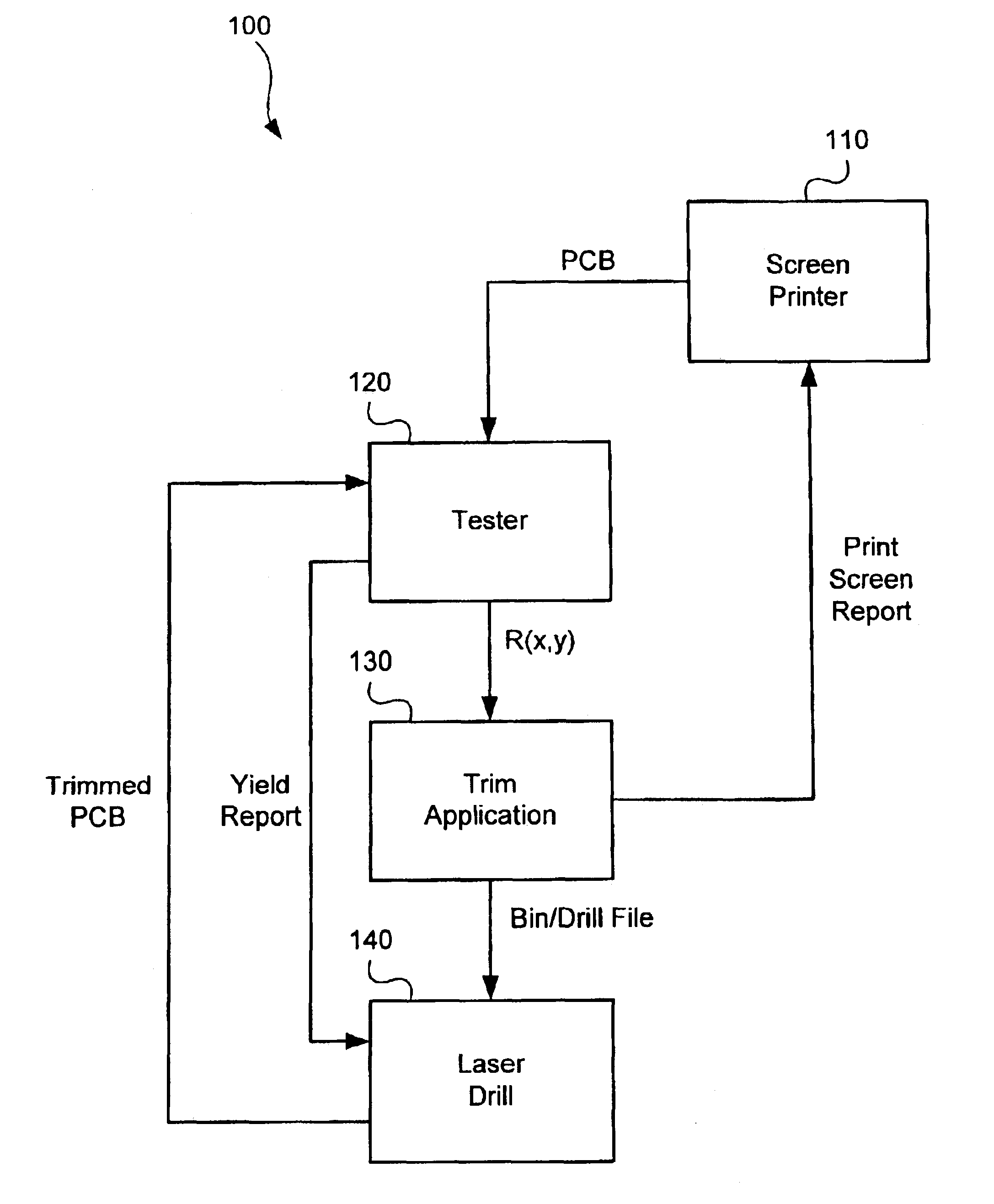
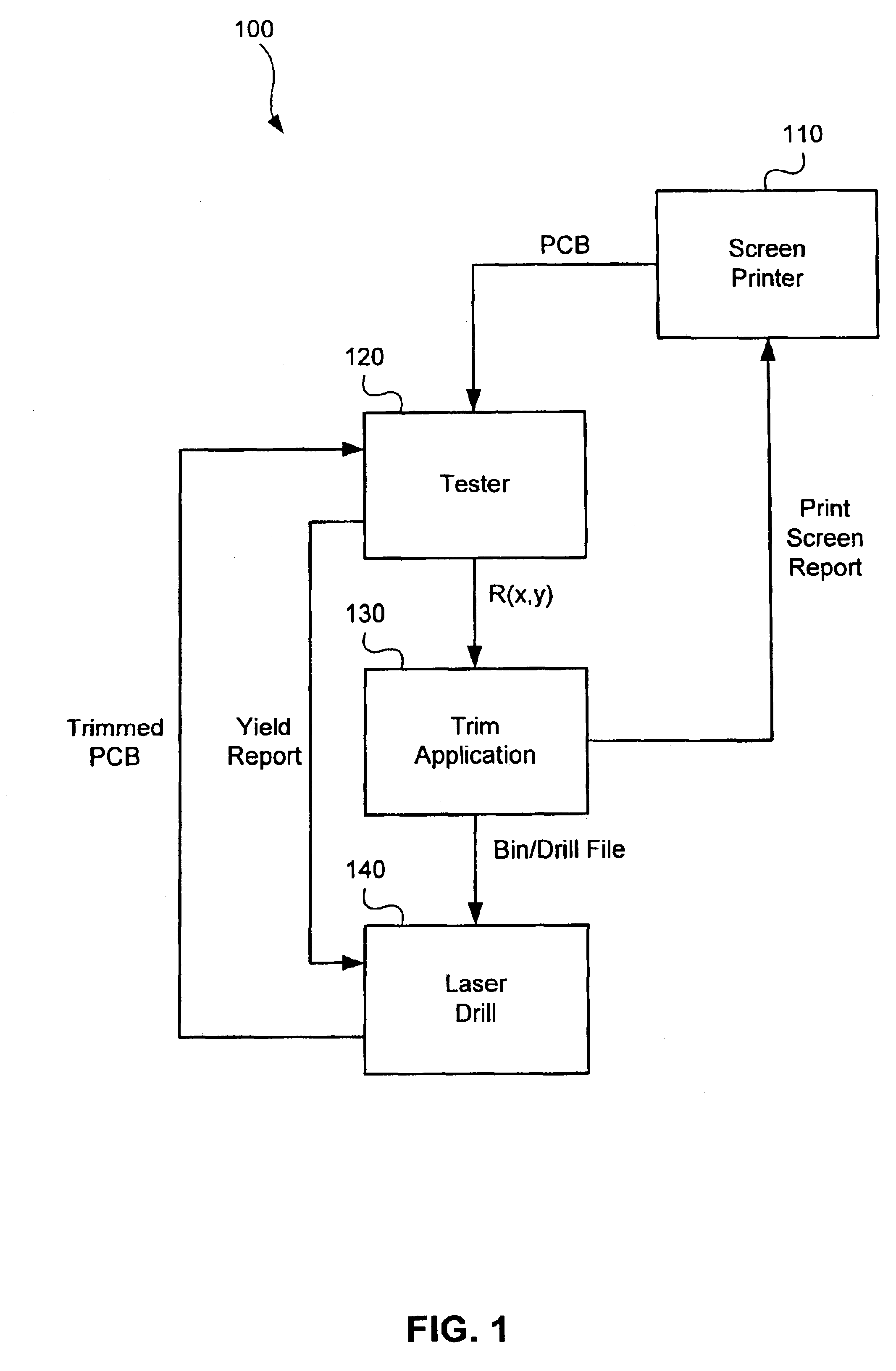
[0018]Referring to FIG. 1, a block diagram of an exemplary system in which the principles of the present invention may be advantageously practiced is illustrated generally at 10...


PUM

PropertyMeasurementUnit
resistanceaaaaaaaaaa
poweraaaaaaaaaa
resistance valueaaaaaaaaaa

Abstract

Improved systems and methods for laser trimming annular resistors printed on a circuit board are provided. An exemplary embodiment measures a resistance value for each annular resistor and sorts the annular resistors into one or more bins based on the measured resistance values and target resistance values associated with each annular resistor. A laser trim file may then be assigned to each bin based on a predictive trim formulation, where each laser trim file defines a set of configuration parameters for a laser drill to conform each annular resistor with their respective target value. The laser drill uses laser trim files to trim the annular resistors within each bin in accordance with a laser trim file assigned to that bin.

Description

BACKGROUND[0001]1. Field of Invention[0002]The present invention generally relates to fabrication of printed circuit boards, and more particularly, to systems and methods for laser trimming of annular passive components fabricated on a printed circuit board.[0003]2. Description of Related Art[0004]Resistors fabricated on the surface of printed circuit boards offer significant electrical performance advantages over surface mount resistors. The problem, however, is that circuit board manufacturers must fabricate these resistors on the circuit board with the desired nominal and tolerance values at the time the circuit board is being manufactured. Because printed resistors are typically buried within the printed circuit board under one or more lamination layers, the circuit board manufacturer is generally unable to correct defects at a later time. The need to properly fabricate resistors the first time for both nominal and tolerance values has been an inhibiting factor for high yield an...

Claims


Application Information

Patent Timeline
Patent Type & Authority Patents(United States)
IPC IPC(8): H01C17/242H05K1/11H05K1/16H05K3/02
CPCH01C17/242H05K1/167H05K1/116H05K3/027H05K2203/171
Inventor BIUNNO, NICHOLASPATEL, ATULOGLE, KENDUDNIKOV, GEORGE
Owner HADCO SANTA CLARA
Why Eureka
Try Eureka