Overlay error model, sampling strategy and associated equipment for implementation

a sampling strategy and overlay error technology, applied in semiconductor/solid-state device testing/measurement, instruments, photomechanical equipment, etc., can solve the problems of inter-field overlay error, overlay error appearance, and factors affecting overlay errors have become increasingly complicated, so as to minimize overlay errors in the microlithographic process

Active Publication Date: 2005-12-13
MACRONIX INT CO LTD
View PDF9 Cites 27 Cited by
  • Summary
  • Abstract
  • Description
  • Claims
  • Application Information

AI Technical Summary

Benefits of technology

[0072]Accordingly, one object of this invention is to provide an overlay model for measuring overlay errors. The overlay model is based on measurable and rectifiable parameters in a correcting system. According to the overlay model, a sampling procedure is also provided so that an optimal sampling strategy is found. Thereafter, according to the parameters and the model, various balancing acts and deductions are executed so that the overlay errors are compensated to within a tolerable range. Ultimately, overlay errors in microlithographic process are minimized.

Problems solved by technology

The appearance of overlay errors can be attributed to intra-field and inter-field errors.
The ‘intra-field overlay error’ refers to the problem caused by a misalignment between a light source filter lens and a mask.
In addition, the so-called ‘inter-field overlay error’ refers to the problem caused by a misalignment between the mask and the wafer.
Due to an increase in threshold dimension and a reduction of feature size in VLSI circuits, factors affecting overlay errors have become increasingly complicated.
The principle factors include system problems, stepper problems, reticle accuracy, linewidth variation and wafer distortion.
However, factors related to stage motion are absent in Perloff's model.
Moreover, lens errors caused by 3-dimensional lens distortion are also considered.
In real applications, such a system is complicated and costly to implement in a common manufacturing facility.
However, conventional models are rarely implemented in production.
Therefore, the parameters in most theoretical models and the actual measured values must be compromised.
In addition, the cost of making overlay measurements and the number of overlay samplings on a wafer are restricted.

Method used


Image

  • Overlay error model, sampling strategy and associated equipment for implementation
  • Overlay error model, sampling strategy and associated equipment for implementation
  • Overlay error model, sampling strategy and associated equipment for implementation

Examples


Embodiment Construction

[0106]Reference will now be made in detail to the present preferred embodiments of the invention, examples of which are illustrated in the accompanying drawings. Wherever possible, the same reference numbers are used in the drawings and the description to refer to the same or like parts.

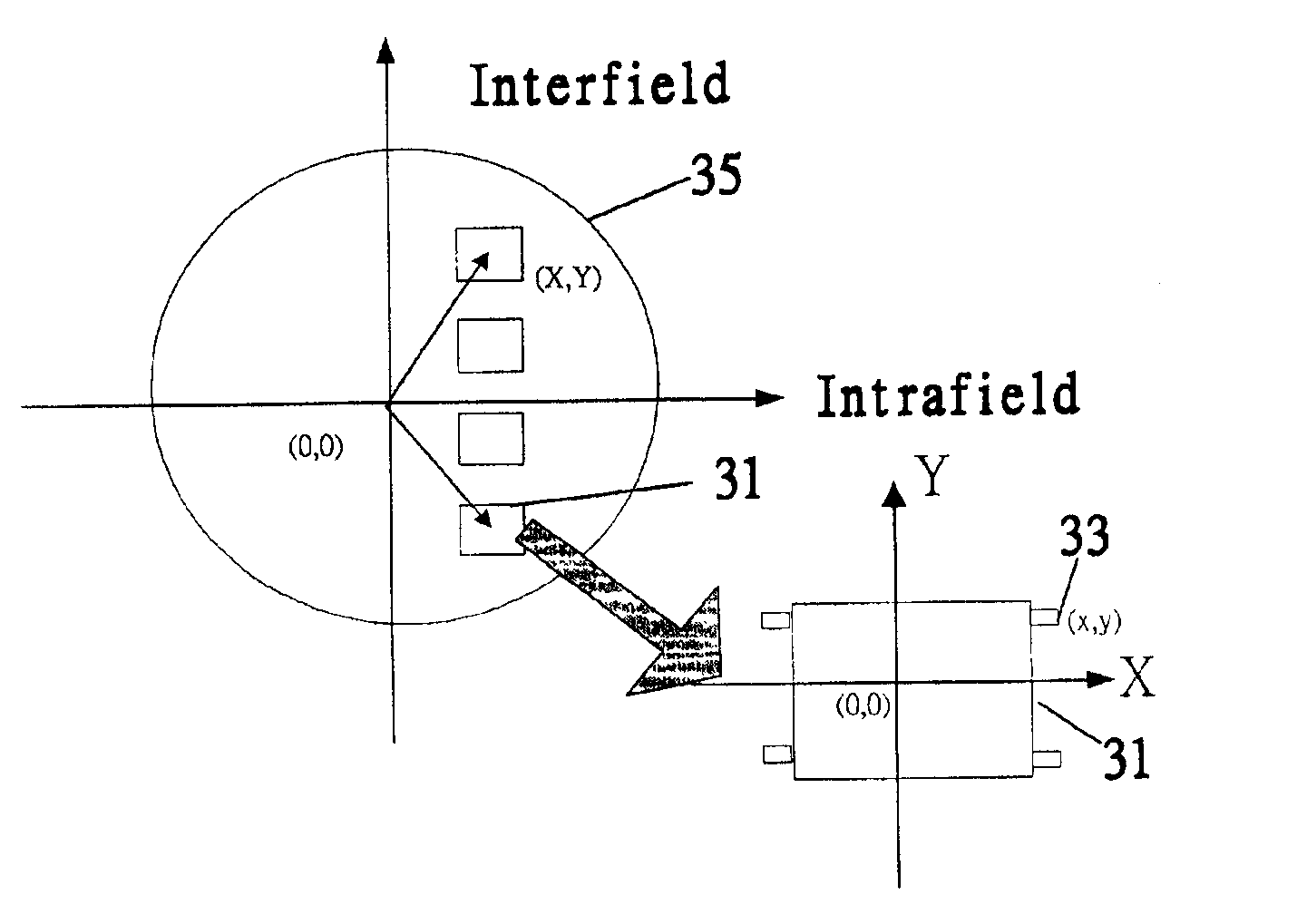
[0107]In this invention, actual measurements by a stepping machine are analyzed to obtain a series of geometric properties of overlay errors such as expansion parameter (E) in the inter-field overlay error pattern. Typically, the overlay error increases towards the edges of a wafer. In addition, for rotation parameter (R), both inter-field and intra-field overlay error patterns include entirely different rotation pattern.

[0108]Hence, for inter-field overlay errors, this invention utilizes actual measurements, simulations and statistics produced by the stepping machine to select four most important parameters including translation (T), magnification (M), rotation (R) and expansion (E). Ultimately, an ...


PUM

PropertyMeasurementUnit
intra-field rotation erroraaaaaaaaaa
inter-field rotation erroraaaaaaaaaa
displacement erroraaaaaaaaaa

Abstract

In the manufacturing of VLSI circuits, production of overlay is a critical step. To obtain a higher resolution and alignment accuracy in microlithographic process, overlay errors must be measured so that overlay errors can be reduced to a tolerable level. This invention provides an overlay error model and a sampling strategy. Utilizing the overlay model and sampling strategy, a device for measuring overlay errors is also designed.

Description

CROSS-REFERENCE TO RELATED APPLICATION[0001]This application claims the priority benefit of Taiwan application serial no. 90104309, filed on Feb. 26, 2001.BACKGROUND OF THE INVENTION[0002]1. Field of Invention[0003]The present invention relates to a method for manufacturing semiconductor devices and the associated equipment required by the method. More particularly, the present invention relates to an overlay error model, a sampling strategy and associated equipment for implementation.REFERENCE ARTICLES[0004]1. Armitage, J. D. and J. P. Kirk, Proceedings SPIE: Integrated Circuit Metrology, Inspection and Process Control II, 921, 207-222 (1988).[0005]2. Arnold, W. H, Proceedings SPIE: Optical / Laser Microlithography, vol. 922, 94-105 (1988).[0006]3. Arnold, W. H, Proceedings SPIE: Optical Microlithography, 394, 87-98 (1983).[0007]4. Brink, M. A., C. G. M. Mol and R. A. George, Proceedings SPIE: Integrated Circuit Metrology, Inspection, and Process Control II, 921, 180-197 (1988).[0008...

Claims


Application Information

Patent Timeline
Patent Type & Authority Patents(United States)
IPC IPC(8): G03F7/20H01L21/66
CPCG03F7/705G03F7/70533G03F7/70633H01L22/20
Inventor CHIEN, CHEN-FUCHANG, KUO-HAOCHEN, CHIH-PINGLIN, SHUN-LI
Owner MACRONIX INT CO LTD
Why Eureka
Try Eureka