
Modular method for manufacturing circuit board

a technology of printed circuit boards and modules, applied in the direction of superimposed coating process, resistive material coating, liquid/solution decomposition chemical coating, etc., can solve the problem of blind vias not being filled, special chemical solutions of a very high cost are needed for the foregoing via filled plating, and serious deviation of the alignment between different circuit layers caused by increased pressing times, etc. problem, to achieve the effect of avoiding serious deviation, reducing the time of heating and pressing processes, and excellent alignmen

Active Publication Date: 2005-12-20
UNITECH PRINTED CIRCUIT BOARD CORP
View PDF7 Cites 12 Cited by
  • Summary
  • Abstract
  • Description
  • Claims
  • Application Information

AI Technical Summary

Benefits of technology

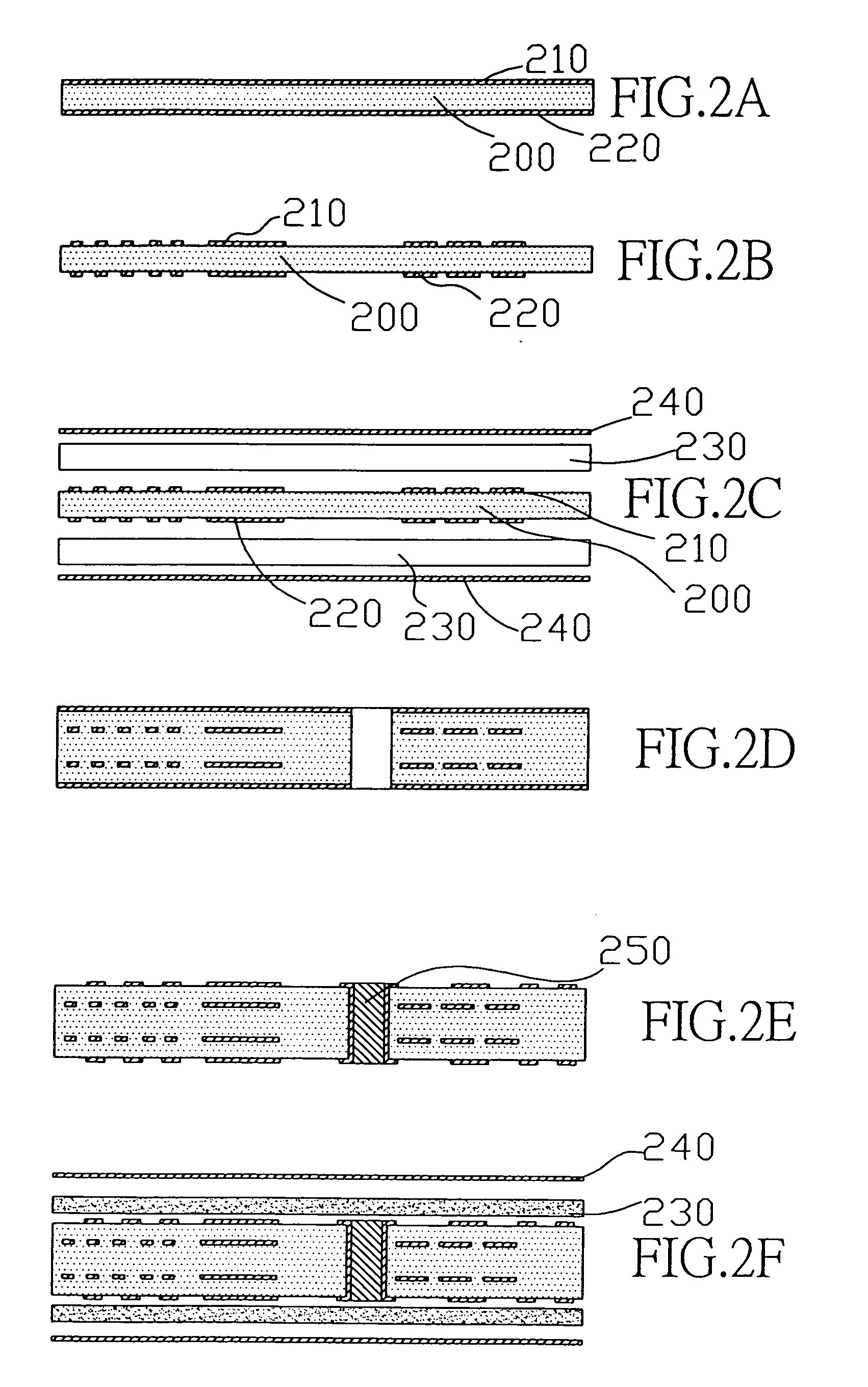
[0019]The primary objective of the present invention is to provide a method for manufacturing multilayer printed circuit boards with blind and buried vias structure by using basic components as the assembly units. The method comprises the steps of producing an electric circuit on the surface of a copper clad laminate by photolithographic and etching methods, pressing a dry film dielectric onto the surface of the laminate by the dry film lamination method after the electric circuit layer is formed, drilling a via by a mechanical drilling method and plugging a plastic conductive material into the via, then removing the coversheet (i.e. a polyester film) on the surface of the dry film dielectric to obtain a basic component. When a multilayer printed circuit board having the blind and buried via structure is manufactured, to comprise the basic components, circuit boards having blind vias and single-sided or double-sided circuits, the dielectric materials and the copper clads according to the required multilayer printed circuit board mode, then heating and pressurization process is performed once to form the multilayer printed circuit boards with blind and buried vias structure. So compare with the prior-art technology that needs layers aligning, pressing and use of special chemical solution for blind via filled plating in each time build up process, the present invention has the following advantages:
[0020]1. Whatever layer counts of multilayer circuit board having blind and buried vias structure, just only once heating and pressurization process is needed to complete the manufacture. The present invention can reduce the times of the heating and pressurization processes. (The prior-art technology requires at least two times of heating and pressurization processes depending on the layer counts of the circuit board structure, and each time takes about 4˜5 hours).
[0022]3. The present invention does not need the special and high cost chemical solution to perform via-filled plating. The present invention directly fills plastic conductive material from the vias of basic components into the blind vias of circuit boards having blind vias and single-sided or double-sided circuits to achieve the same effect as the via-filled plating, and save much time and cost.
[0023]4. Unlike the prior-art technology that needs to make the circuit board layer by layer, continuously repeat build up process from the inner layers to the outer layers (heating and pressurization, mechanical drilling, laser drilling, via-filled plating . . . etc.), the present invention separately manufacture the basic components and the circuit boards having blind vias and single-sided or double-sided circuits then select the good ones to perform once heating and pressurization. So the present invention not only save the overall manufacturing time, but also enhance the yield rate and lower the cost of fault at a later stage of the manufacturing process.

Problems solved by technology

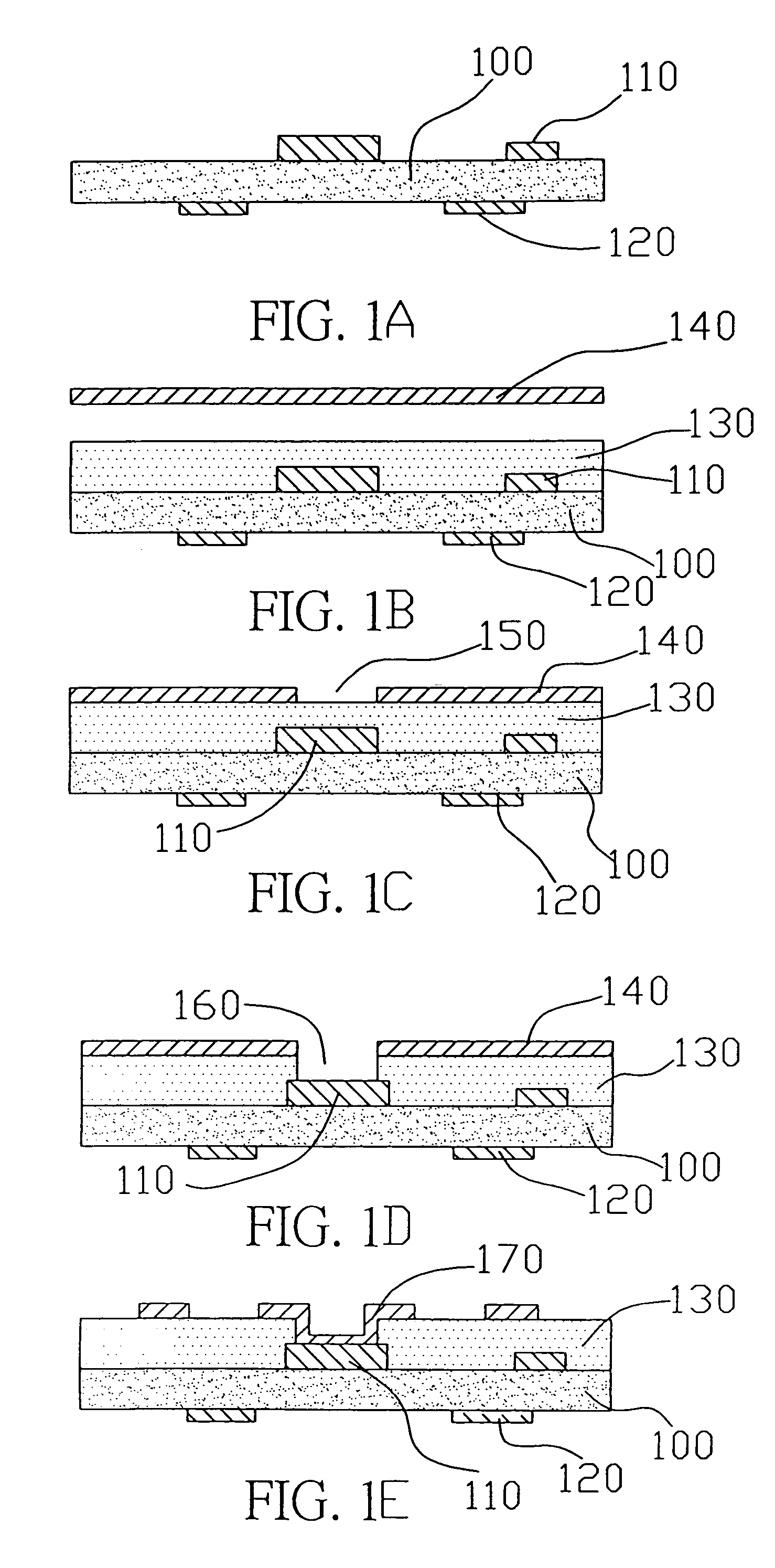
However, it is noteworthy that the plated metal can just be deposited along the sidewall of the via (as indicated by 170 in FIG. 1E) in traditional plating, and the blind via cannot be filled.
Therefore, a special chemical solution of a very high cost is needed for the foregoing via filled plating to achieve the purpose of filling the via by plating.
Further, the prior-art technology requires a pressing process each time for adding a layer.
Since each pressing can only confirms the alignment between a new circuit layer and its next circuit layer, therefore a serious deviation on the alignment between different circuit layers caused by the increased times of pressings will be resulted.
From the foregoing process, it is obvious that the prior-art process takes long time, not only is difficult to enhance the yield rate, but also increase the cost of fault at a later stage of the manufacturing process.

Method used


Image

  • Modular method for manufacturing circuit board
  • Modular method for manufacturing circuit board
  • Modular method for manufacturing circuit board

Examples


Embodiment Construction

[0033]The present invention relates to a modular method for manufacturing circuit boards by using basic components as the assembling units to produce multilayer circuit boards having the blind and buried vias structure.

[0034]Please refer to FIGS. 3A to 3E for the illustrative views of producing a basic component of the present invention. The method comprises the steps of using an electric circuit manufacturing process to produce an electric circuit layer 11, 12 on the surface of a copper clad laminate 10 by photolithographic and etching methods (as shown in FIG. 3A); pressing a dry film dielectric 20 which at B-stage (i.e. the stage of a resin before its reaching a glass conversion state) and having a coversheet (i.e. a polyester film) onto the electric circuit layer 11, 12 by the dry film lamination method (as shown in FIG. 3B); and drilling vias 13 at predetermined position by mechanical drilling method (as shown in FIG. 3C) and plugging plastic conductive material 30 into the via...


PUM

PropertyMeasurementUnit
timeaaaaaaaaaa
electricaaaaaaaaaa
conductiveaaaaaaaaaa

Abstract

The present invention discloses a modular method for manufacturing circuit boards, which is a method of manufacturing multilayer printed circuit boards with blind and buried vias structure by using basic components as the assembly units. The method comprises the steps of producing electric circuits on the surface of a copper clad laminate by photolithographic and etching methods, pressing a dry film dielectric onto the surface of the laminate by the dry film lamination method after the electric circuit layer is formed, drilling a via and plugging a plastic conductive material into the via to obtain a basic component. When a multilayer printed circuit board having the blind and buried via structure is manufactured, the basic component serves as an assembling unit to stack with other circuit board having blind via and single-sided or double-sided electric circuits according to the multilayer circuit board mode to perform a heating and pressurization procedure and form a multilayer circuit board with blind and buried via structure. Such arrangement not only saves the time for aligning layers, pressing and blind via filled plating of the prior-art technology, but also enhances the yield rate and reduces the failure cost.

Description

BACKGROUND OF THE INVENTION[0001]1. Field of the Invention[0002]The present invention relates to a modular method for manufacturing printed circuit boards, which is a method of manufacturing multilayer printed circuit boards with blind and buried vias structure by using basic components as the assembly units. The method adopts a dry film lamination method to press a dry film dielectric (i.e. a dielectric material in the form of a dry film, which is a semi-sticky plastic state) at B-stage (i.e. the stage of a resin before its reaching a glass conversion state) onto a laminate after the photolithography and etching processes are performed. Vias are drilled at appropriate positions on the upper and lower layers that require an electric connection, and then a plastic conductive material is filled into the vias to produce basic components. To comprise the basic components, circuit boards having blind vias and single-sided or double-sided circuits, the dielectric materials and the copper ...

Claims


Application Information

Patent Timeline
Patent Type & Authority Patents(United States)
IPC IPC(8): H01K3/10H05K3/40H05K3/46
CPCH05K3/462H05K3/4069H05K3/4623H05K3/4652H05K2201/0394Y10T29/49117H05K2201/096H05K2203/0191Y10T29/49155Y10T29/49126Y10T29/49165H05K2201/09509
Inventor HSIEN, CHOU CHENG
Owner UNITECH PRINTED CIRCUIT BOARD CORP
Learn More