Stamp device for printing a pattern on a surface of a substrate

a stamp device and substrate technology, applied in the field of stamp devices for printing patterns on substrate surfaces, can solve the problems of small thermal or mechanical expansion, inability to meet runout, defective and inaccurate stamping, etc., and achieve the effect of severely reducing the capability to compensate substrate topography and stamp thickness inhomogeneities

Inactive Publication Date: 2005-12-20
IBM CORP
View PDF13 Cites 26 Cited by
  • Summary
  • Abstract
  • Description
  • Claims
  • Application Information

AI Technical Summary

Benefits of technology

[0017]A conventional thin film hybrid stamp provides a carrier layer like a flat metal sheet or a thin glass foil onto which one side the patterned layer made of stamp material like PDMS is attached. The carrier layer is rigid in its plane but flexible perpendicular to its plane. The underlying idea of the invention is to contact the other side of the rigid carrier layer with a layer made of a softer material than the patterned layer, at least while contacting the stamp device with the to be printed surface of the substrate. During printing a load acts onto the stamp, which is directed through the soft layer onto the backside of the rigid carrier layer. Under this condition, the soft layer absorbs the majority of the pressure difference created by the load acting on inhomogeneous built stamps or by substrate warp without overloading the stamp pattern. A second effect is the larger contact area between the stamp and the substrate that distributes the added printing force. Tests showed that the local leveling effect of the soft layer is more effective the thinner the rigid carrier layer is.
[0025]The before described press means are characterized by a rigid surface due to the fact that the soft layer is already provided onto the backside of the rigid carrier layer of the stamp device. The second and fourth inventive embodiment of the stamp device for printing a pattern on a surface of a substrate comprises also a two-sided rigid carrier.layer providing on its first side a patterned layer made of a first material but its second side still remains rigid, no soft layer is attached like in the first case. Rather a contact means is provided for contacting the second side of said carrier layer by applying a force onto said stamp. The contact means for example in the form of a roller or cylinder element has at least one soft layer at its outer contour being of softer material than said first material of said patterned layer. Such roller element has a cylindrical shape providing the soft layer at its superficies and contacts the stamp device in a propagating contact front while unrolling at the backside of the rigid carrier layer of the stamp device. The loading force of the roller or cylinder element on the stamp device and substrate can be varied corresponding to the stamp patterns to yield best print results. The roller or cylinder with a soft surface layer further allows to compensate for variations in stamp thickness and substrate topography. To prevent sliding of the stamp on the cylinder or sliding of the roller on the stamp a good friction between the soft layer and the hard surface is ensured if there is a friction coefficient between the soft layer and the rigid carrier layer of about 0.5-1.
[0032]In case transluminescent materials are used for the stamp device as well as for the substrate the printing arrangement can be illuminated with a sensing light for detecting contact areas between the stamp and the substrate while printing. With this technique an online control of the printing process can be carried out which improves the yield and ensures the printing accuracy and quality. When either substrate or stamp are transluminescent, a similar sensing circuit can be implemented that relies on detection of reflected light instead.
[0034]In a first way support structures, like posts or lines, are provided at the patterned layer in said areas free of structures for preventing said areas free of structures from sagging and contacting said substrate by applying a load onto said stamp device. Unavoidable by using these support structures are local contacts between the stamp device and the substrate in areas in which contacts should have been avoided. However support structures lead to controlled prints at the surface of the substrate which can be arranged apart from the main desired printing pattern without interfering said pattern.
[0035]Such support structures shall provide maximally the same structure depth as the patterned structures at the patterned layer and being preferably of the same material or of harder material like poly methyl methacrylate (PMMA). In case a different material is used for the support post the ink transfer efficiency on these patterns from the inking solution to the substrate surface can be reduced in order to minimize the printing traces left by those support posts. The overall transfer efficiency can be reduced by (i) treating the support post surface to make it reject the ink during the inking process or (ii) by treating the support post surface to retain the ink during the printing process.
[0039]Also it is possible to insert a gaseous medium through the passage channels into the cavities to establish a controlled overpressure in said cavities for preventing sagging by application of a load onto said stamp device.

Problems solved by technology

These stresses before or during printing can deform the stamp or cause parts of it to collapse, which leads to defective and inaccurate prints.
The diverging demands given by conformability, high pattern stability, small thermal or mechanical expansion, and runout cannot be met by one material alone but require layered structures.
Very thin polymer layers (<0.1 mm) reduce this problem but suffer from a severely reduced capability to compensate substrate topography and stamp thickness inhomogeneities.
Nevertheless a couple of problems still remain for producing large area printed structures on substrates using soft lithography technique:The larger the to be printed area the greater the possibility of inclusion of air bubbles in the contact plane between the patterned stamp layer and the to be printed surface.
For instance, printing of a flat full wafer having a slight bow causes inclusion of air bubbles frequently leading to zones of failed printing due to missing contact between the stamp and the wafer surface.Inhomogeneities of the thickness of the thin film hybrid stamp due to chemical or thermal shrink and tolerances in the printing tool cause uneven load on different areas of the stamp.
This leads to collapse of patterns and / or sagging.In connection with the before mentioned disadvantage there exists no possibility for control or monitoring the actual surface-distributed load acting onto the stamp while printing to locate printing zones in which ceiling or bottom load limits are exceeded or not even reached.
Monitoring local force distribution at the contact layer between the stamp and surface however could allow a post-print analysis thus improves the process of soft lithography noticeably.For providing an accurate alignment between the patterned layer of the stamp and the surface to be printed difficulties can arise in printing large surfaces due to inherent differences of expansion or stretch conditions of the contacting surfaces.
Repeated conformal printing of different sets of structures onto a surface inevitably leads to deviations of positioning the stamp towards the surface between each printing event.Disturbing print contacts between the stamp and the substrate appear in areas of the patterned layer where no structured pattern is provided.
If the distance of two neighboring patterned structures is large enough sagging of the receded patterned layer appears from a distinct load of the stamp leading to unintentional prints.

Method used


Image

  • Stamp device for printing a pattern on a surface of a substrate
  • Stamp device for printing a pattern on a surface of a substrate
  • Stamp device for printing a pattern on a surface of a substrate

Examples


Embodiment Construction

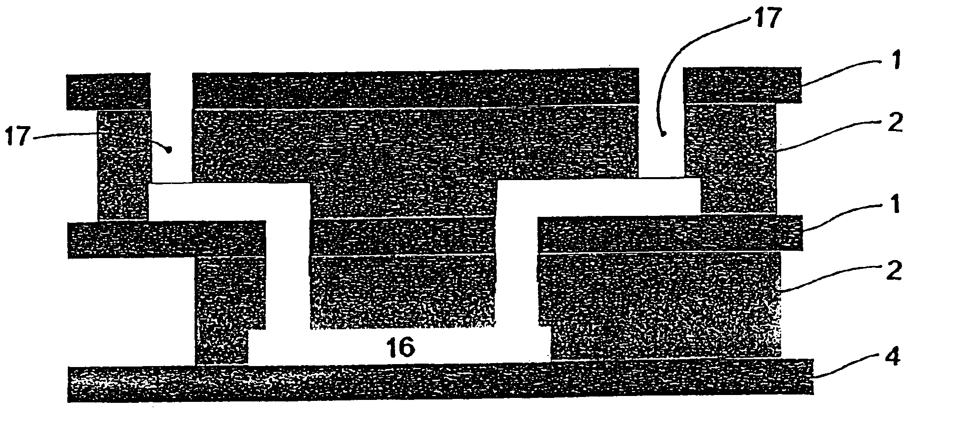
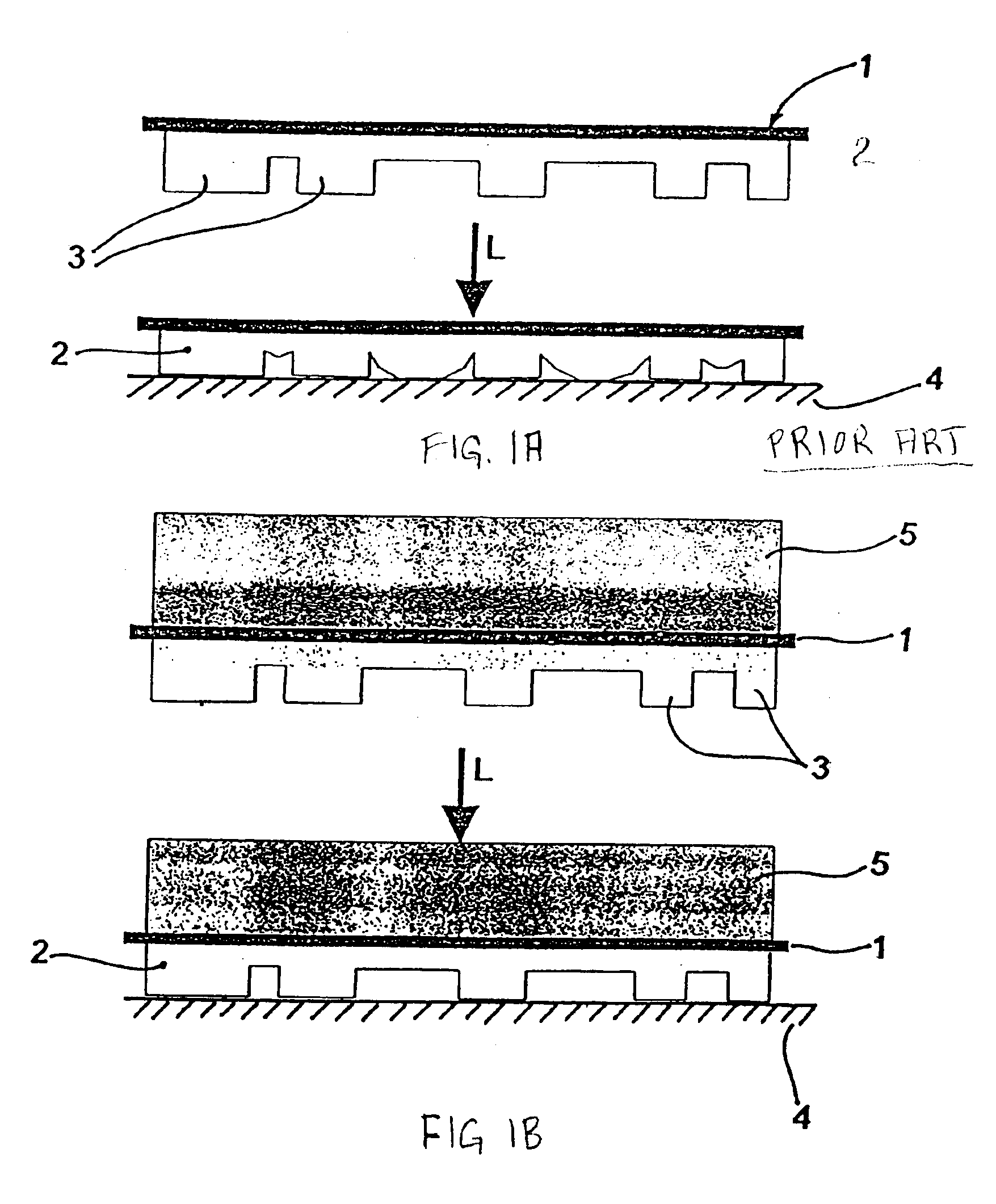
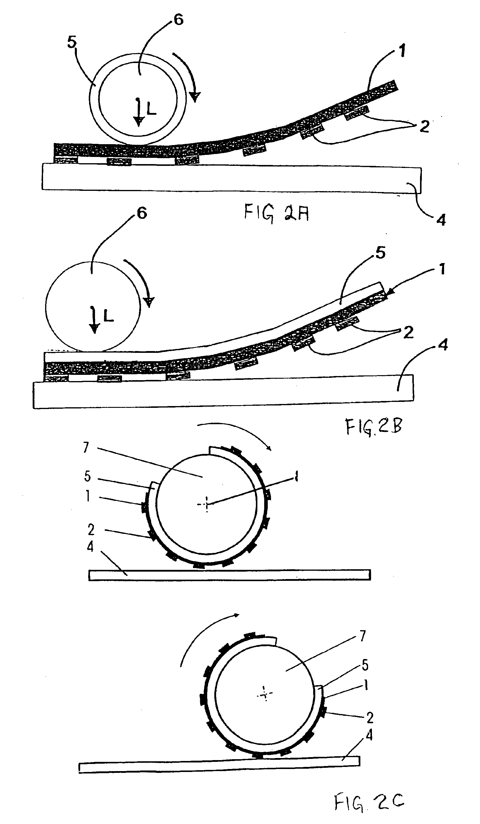
[0059]FIG. 1 shows a conventional stamp device having a backplane or in terms of this disclosure a carrier layer 1 typically made of a metal foil or a thin glass or quartz plate. On its one side a patterned layer 2 is applied having patterned structures 3 which are moistened at least on its lower side with an ink or a chemical or biological substance which shall be transferred to the surface of a substrate 4 by a printing process. While printing, the stamp device is pressed under a load L against the surface of a substrate 4 as illustrated in FIG. 1A lower sketch. Due to mechanical compression caused by uneven distribution of the load L onto the stamp, deformation appears and squeezes the pattern structures 3 and creates sagging in non supported regions.

[0060]When using a soft pattern 5 which is attached at the other side of the carrier layer 1 as it is shown in FIG. 1B no sagging appears under load. The soft layer 5 absorbs the deformation by distributing the load and leaves the pa...


PUM

PropertyMeasurementUnit
thicknessaaaaaaaaaa
radiusaaaaaaaaaa
friction coefficientaaaaaaaaaa

Abstract

A stamp device for printing a pattern on a surface of a substrate having a two-sided rigid carrier layer providing on its first side a patterned layer made of a first material and being combined on its second side with a soft layer made of a softer material than that of the first material.

Description

FIELD OF THE INVENTION[0001]The present invention relates to a stamp device for printing a pattern on a surface of a substrate.BACKGROUND OF THE INVENTION[0002]Soft lithography, a known technique for transferring micro patterns onto a surface of a substrate serving as the basic structure for integrated circuits, (see also Xia, Y.; Whitesides, G. M. Angew. Chem. Int'l. Ed. 1998, 37, 550) relies on a stamp to bring a reactant in contact with a substrate.[0003]Stamp materials in soft lithography are exposed to capillary forces, self-adhesion, and mechanical stresses during printing. These stresses before or during printing can deform the stamp or cause parts of it to collapse, which leads to defective and inaccurate prints. Most of the work on contact printing has been done using Sylgard 184 manufactured by Dow Corning Corp., Midland, Mich., USA, a commercially available thermo-cured Siloxane polymer, whose structures smaller than 1 μm tend to merge or collapse during inking and printi...

Claims


Application Information

Patent Timeline
Patent Type & Authority Patents(United States)
IPC IPC(8): B41K1/02B41K3/00B41K3/04B41M1/02B41N10/04G03F7/00
CPCB82Y10/00B41K1/22G03F7/0002B82Y40/00B41M1/02B41K3/00
Inventor BRUNO, MICHELSCHMID, HEINZDELAMARCHE, EMMANUELBIETSCH, ALEXANDER
Owner IBM CORP
Why Eureka
Try Eureka