

Light emitting element and method of making same
a technology of light emitting elements and methods, applied in the direction of polycrystalline material growth, chemistry apparatus and processes, crystal growth process, etc., can solve the problems of micro-pipe defects penetrating vertically, light emitting elements employing sic substrates, and poor crystalline quality of sic single crystal wafers, etc., to achieve good manufacturing efficiency
- Summary
- Abstract
- Description
- Claims
- Application Information
AI Technical Summary
Benefits of technology
Problems solved by technology
Method used
Image

Examples
example 1
Forming of n-GaN Thin Film on p-type Conductivity Substrate
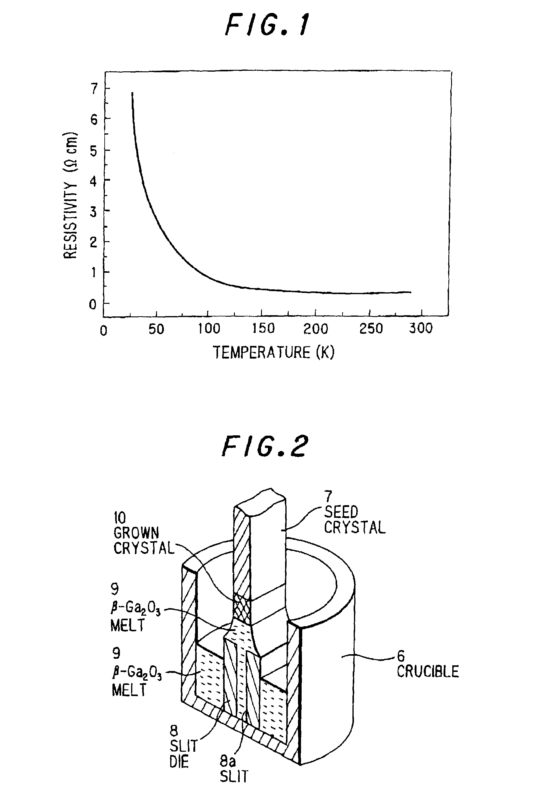
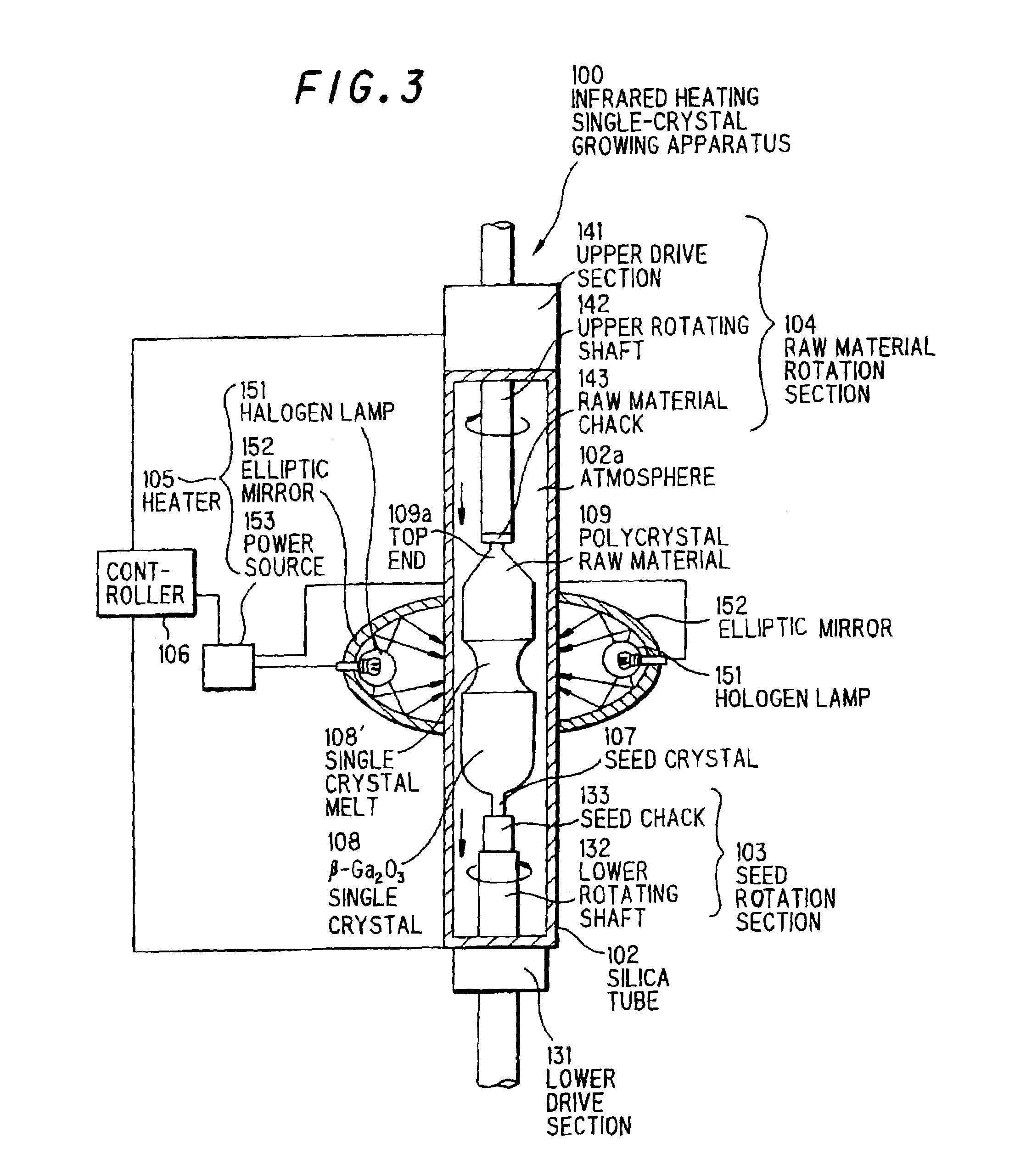
[0086]The p-type conductivity substrate is made as follows. First, β-Ga2O3 single crystal is prepared by FZ method. The β-Ga2O3 polycrystalline raw material is obtained by uniformly mixing, for example, β-Ga2O3 including MgO (p-dopant source) and charging a predetermined amount of the mixture into a rubber tube, cold-compressing it at 500 MPa to form a stick, then sintering it at 1500° C. for ten hours in the atmosphere. Thereby, β-Ga2O3 system polycrystalline raw material including Mg is obtained. By another way, β-Ga2O3 seed crystal is provided. Under the growth atmosphere with total pressure of 1 to 2 atm, flowing mixture gas of N2 and O2 at 500 ml / min, the β-Ga2O3 seed crystal and β-Ga2O3 system polycrystalline raw material are contacted to each other in the silica tube, and they are heated such that the β-Ga2O3 seed crystal and β-Ga2O3 system polycrystalline raw material are melted at the contacting portion. The melting...
example 2
Light Emitting Element with pn-Junction
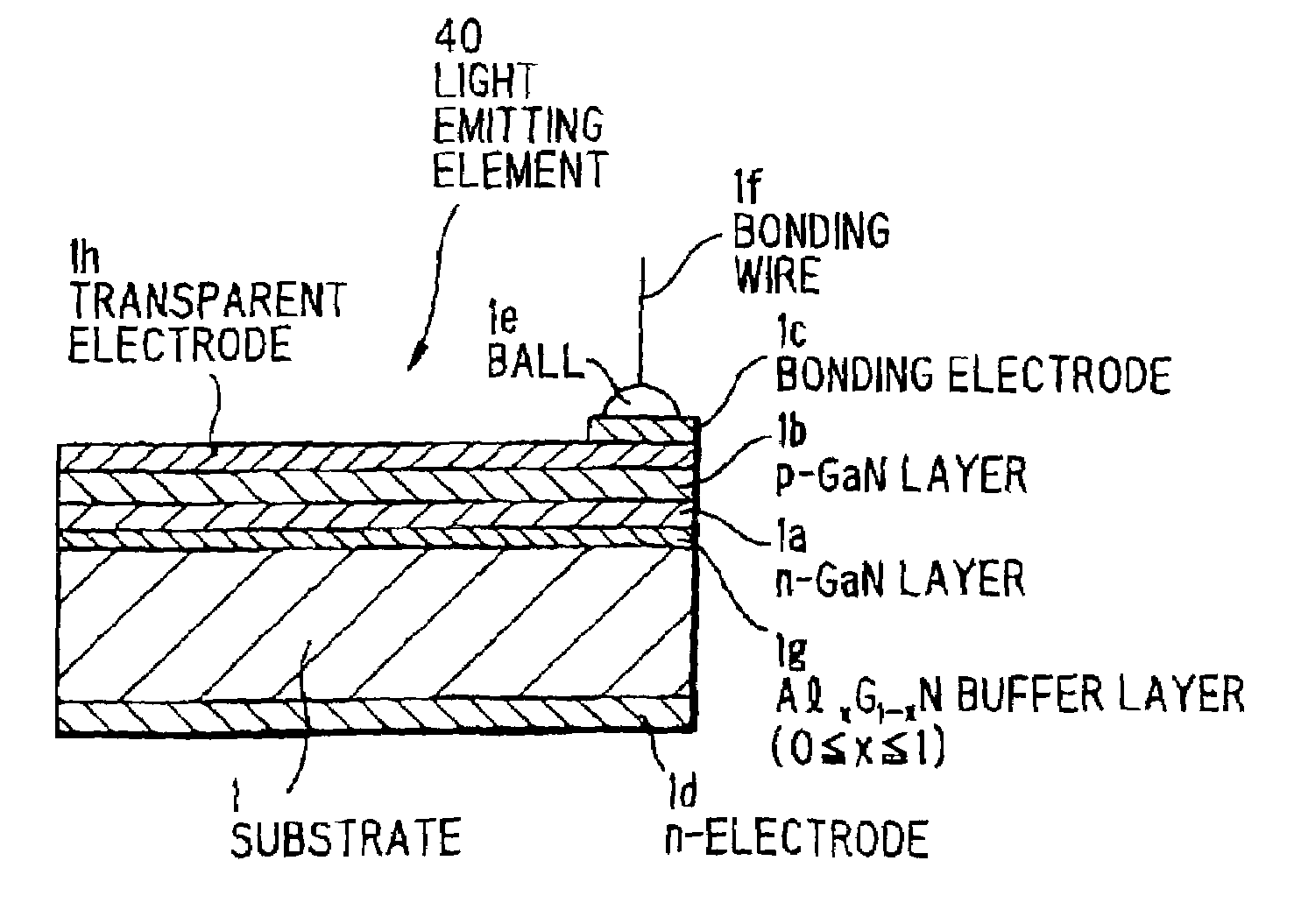
[0088]FIG. 9 shows a light emitting element with pn-junction mounted on a printed circuit board. The light emitting element 40 includes: a Ga2O3 substrate 41 of β-Ga2O3 single crystal: a AlXGa1−XN buffer layer 42 (0≦x≦1) formed on the Ga2O3 substrate 41; a n-GaN layer 43 formed on the AlXGa1−XN buffer layer 42; a p-GaN layer 44 formed on the n-GaN layer 43; a transparent electrode 45 formed on the p-GaN layer 44; a Au bonding electrode 47 formed on part of the transparent electrode 45; and a n-electrode 46 formed on the bottom surface of the Ga2O3 substrate 41. The light emitting element 40 is mounted on the printed circuit board 50 through a metal paste 51 and a bonding wire 49 is bonded to the bonding electrode 47 while forming a ball 48.
[0089]The light emitting element 40 emits light at the pn-junction interface where the n-GaN layer 43 and p-GaN layer 44 are bonded. Emitted light is output such that part of emitted light is output, as outpu...
example 3
Flip-Chip Type Light Emitting Element
[0090]FIG. 10 shows a flip-chip type light emitting element. The light emitting element 40 includes: a Ga2O3 substrate 41 of β-Ga2O3 single crystal; a AlXGa1−XN buffer layer 42 (0≦x≦1) formed on the Ga2O3 substrate 41; a n-GaN layer 43 formed on the AlXGa1−XN buffer layer 42; a p-GaN layer 44 formed on part of the n-GaN layer 43; a n-electrode 46 formed on the n-GaN layer 43; and a p-electrode 52 formed on the p-GaN layer 44. The light emitting element 40 is flip-chip bonded through solder balls 63, 64 beneath the p-electrode 52 and n-electrode 46 to lead frames 65, 66.
[0091]The light emitting element 40 emits light at the pn-junction interface where the n-GaN layer 43 and p-GaN layer 44 are bonded. Emitted light is output, as output light 60, upward transmitting through the Ga2O3 substrate 41.
PUM
 Abstract
Description
Claims
Application Information