Stacked packages

a technology of stacking packages and circuit boards, applied in the direction of printed circuit aspects, sustainable manufacturing/processing, final product manufacturing, etc., can solve the problems of limiting the speed of circuit operation, requiring appreciable time for signal propagation, and traces on circuit boards typically have significant length and impedan

Inactive Publication Date: 2005-12-20
TESSERA INC
View PDF154 Cites 168 Cited by
  • Summary
  • Abstract
  • Description
  • Claims
  • Application Information

AI Technical Summary

Benefits of technology

[0012]The dielectric layer in each circuit panel may have a disconnection aperture or opening, and the interruptions in the branches of the multi-branch traces may be formed at such disconnection apertures. The disconnection apertures can be formed in the dielectric layers when the units are manufactured or when the branches are interrupted, typically at a later stage in the process. In one arrangement, the circuit panel of each unit has edges, and the disconnection apertures are provided in the form of notches extending inwardly from one or more of the edges. The terminals of such a unit may include an outer row disposed adjacent to an edge of the circuit panel and the branches of the multi-branch traces may have portions extending outwardly to or beyond the outer row of terminals. In this instance, the notches need not extend inwardly beyond the outer row of terminals, so that the interruptions in the multi-branch leads can be formed readily.
[0013]Alternatively, or in combination with the above, the branches of a multi-branch trace may define gaps such that the gaps intervene between the common section of the multi-branch trace and the select terminals associated with the various branches. Selective connections may be formed across such one or more of the gaps by conductive elements such as wire bonds or solder masses so as to connect one or of the select terminals to the common section. For example, the gaps can be bridged using solder applied in the package assembly plant with the same equipment as is used to form vertical buses between the various units. Here again, the various units may be identical to one another until the time the solder is applied, thus simplifying handling and stocking of the units.
[0022]In one arrangement, the traces of each unit extend along the first surface of the dielectric layer in that unit, and the front surface of the chip in each unit faces toward the second surface of the dielectric layer in that unit. In a chip assembly of this type, at least some of the units desirably include heat transfer layers overlying the traces of such units, and these units bear on one another through the heat transfer layers. Thus, the heat transfer layer of each such unit desirably abuts the rear surface of the chip in the next adjacent unit. The heat transfer layers of these units desirably extend across the bond windows in the dielectric layers of these units and are substantially flat, at least in the region extending across the bond windows. Such units desirably further include an encapsulant at least partially filling the bond windows. During manufacture, the heat transfer layers may serve as masking layers which confine the encapsulant so that the encapsulant does not protrude beyond the dielectric layer. As further discussed below, the flat heat transfer layers allow close engagement of the units with one another and good thermal contact between adjoining units. These features contribute to the low height of the assembly and promote effective heat dissipation from chips within the assembly.
[0024]A chip assembly according to another aspect of the invention also includes a plurality of units. Each unit includes a circuit panel and may include one or more chips. Each circuit panel has a number of terminals and traces extending on or in the panel. The traces are electrically connected between the contacts of the one or more chips and the terminals. The units are superposed on one another in a stack. A plurality of conductive masses are disposed between the terminals of the units and connect the terminals of the adjacent units to one another forming vertical buses. The top-most unit includes one or more termination elements, and desirably an array of plural termination elements, such that one, or more, signals, received from one, or more, of the vertical buses are electrically terminated. The termination elements desirably provide electrical characteristics at the upper ends of the vertical buses which mitigate signal reflection along the buses.
[0026]A chip assembly according to yet another aspect of the invention also includes a plurality of units. Each unit includes a circuit panel and may include one or more chips. Each circuit panel has a number of terminals and traces extending on or in the panel. The traces are electrically connected between the contacts of the one or more chips and the terminals. The units are superposed on one another in a stack. A plurality of conductive masses are disposed between the terminals of the units and connect the terminals of the adjacent units to one another forming vertical buses. A plurality of the vertical buses around at least a portion of the periphery of the chip assembly are connected to ground or to another source of constant potential. These busses cooperatively define a Faraday cage around at least a part of the periphery of the stacked assembly. Preferably, the top-most unit includes a conductive plane such as a ground plane. These vertical buses constituting elements of the Faraday cage desirably are connected to the conductive plane so that the conductive plane forms a part of the Faraday cage. A stacked assembly in accordance with this aspect of the invention provides economical electromagnetic shielding.

Problems solved by technology

The traces on the circuit board typically have significant length and impedance so that appreciable time is required for propagation of signals along the traces.
This limits the speed of operation of the circuit.
However, providing a circuit with individual select connections in a stacked package introduces additional complexities.
This need for customization of the units adds complexity to the manufacturing process.
This arrangement inherently requires a relatively large chip carrier, which adds to the cost and bulk of the package.
This, again, adds to the cost and complexity of the manufacturing process.

Method used


Image

  • Stacked packages
  • Stacked packages
  • Stacked packages

Examples


Embodiment Construction

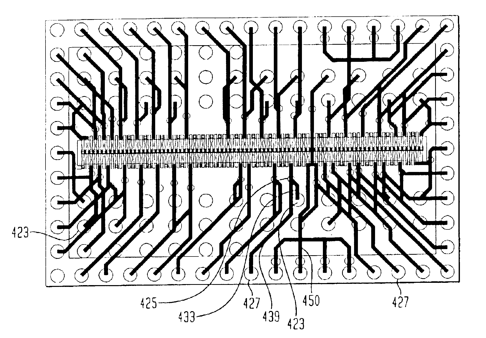
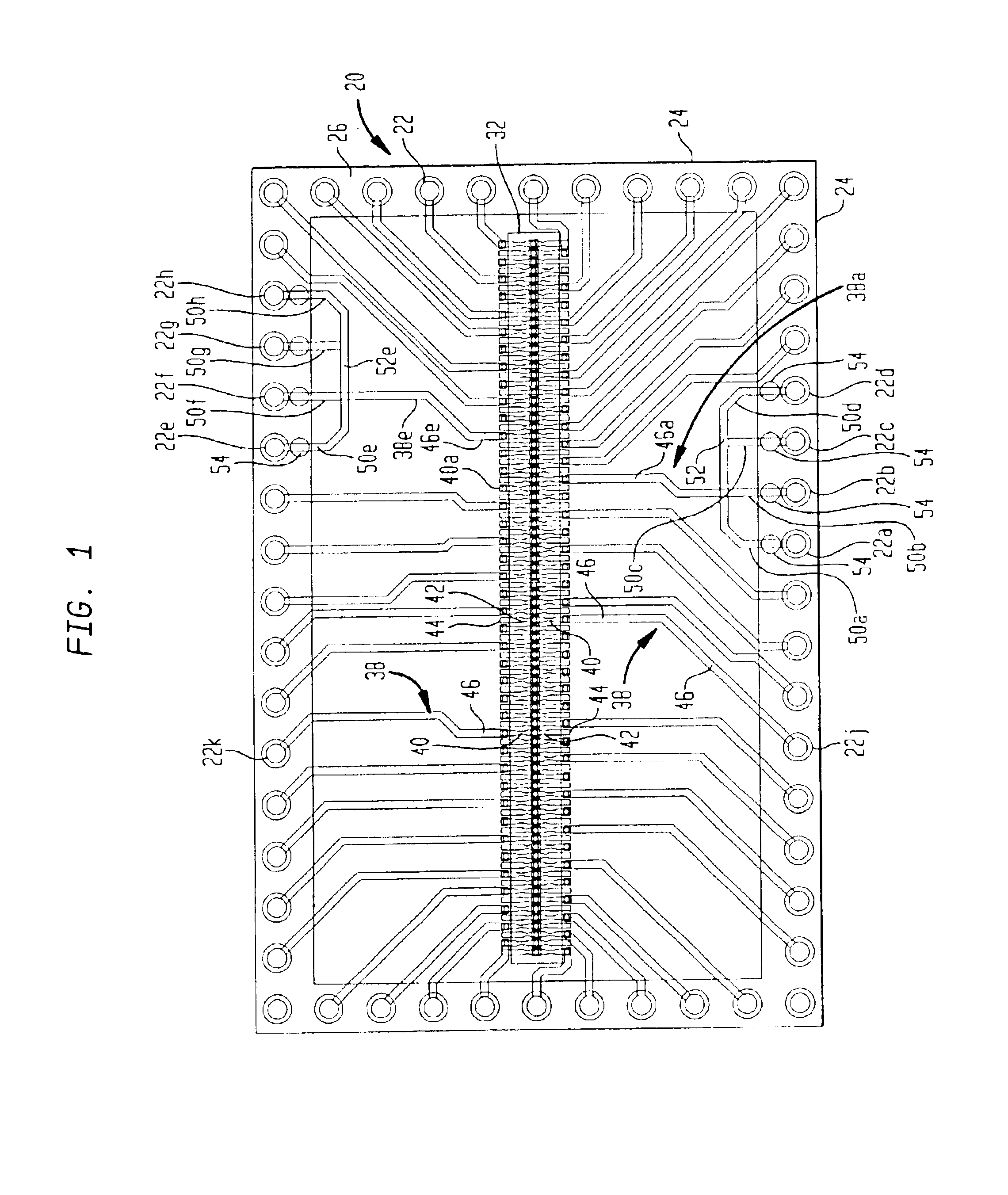
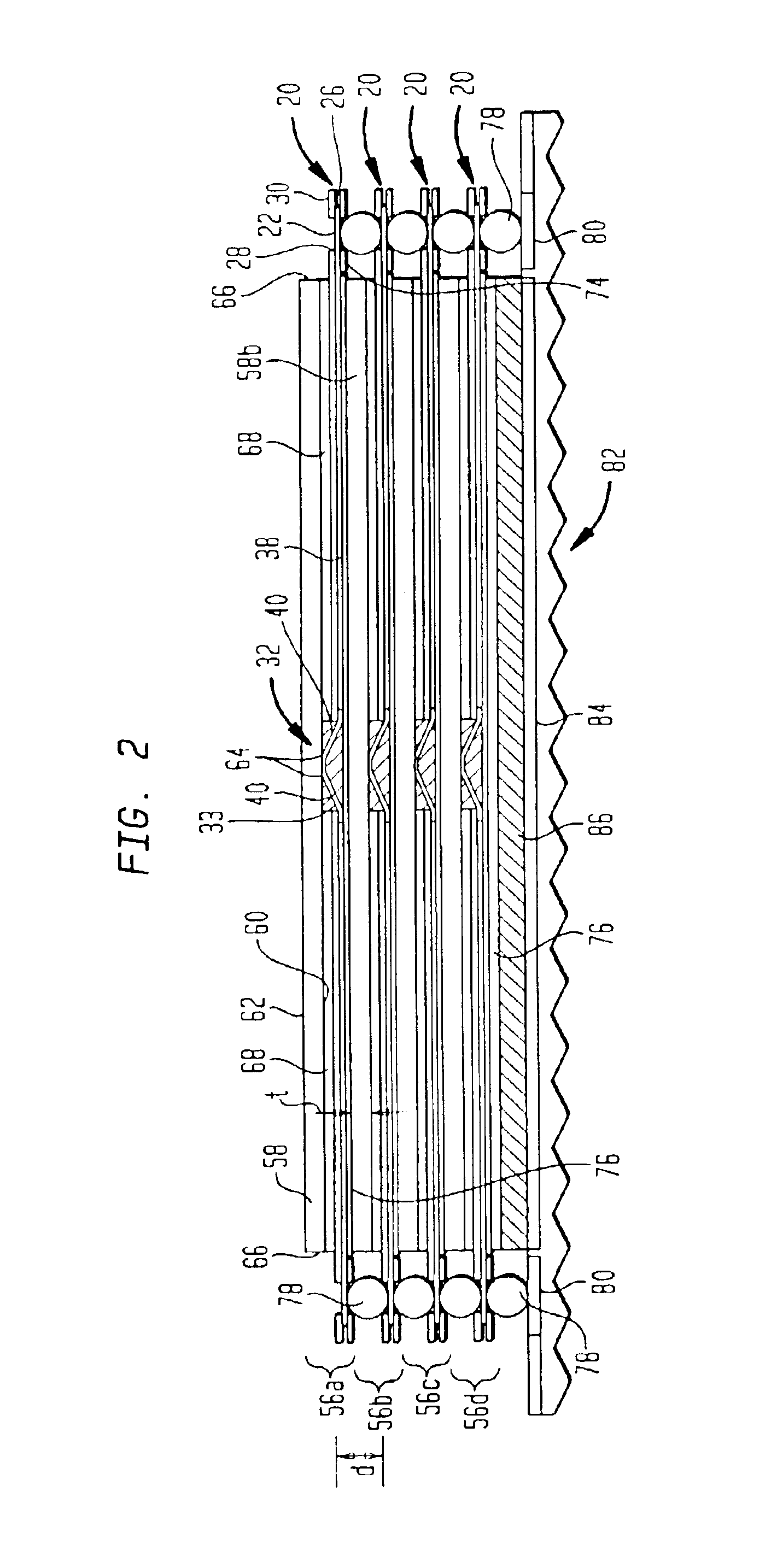
[0062]A package in accordance with one embodiment of the invention uses a plurality of package elements 20, each such element being in the form of a circuit panel. Each such circuit panel may include a dielectric layer in the form of a thin, flexible dielectric tape as, for example, a layer of reinforced or unreinforced polyimide, BT resin or the like on the order of 25-100 μm thick, most preferably 25-75 μm thick. Alternatively, each panel may include a dielectric such as a fiberglass-reinforced epoxy as, for example, an FR-4 or FR-5 board. The panel has numerous terminals 22 disposed in rows within a peripheral region of the panel, adjacent the edges 24 of the panel. In the embodiment illustrated, rows of terminals are provided along all four edges. However, the terminals can be provided adjacent less than all of the edges as, for example, in two rows adjacent to two opposite edges of the panel. Each terminal 22 may be in the form of a flat, relatively thin disc of copper or other...


PUM


Abstract

A stacked chip assembly includes individual units having chips mounted on dielectric layers and traces on the dielectric layers interconnecting the contacts of the chips with terminals disposed in peripheral regions of the dielectric layers. At least some of the traces are multi-branched traces which connect chip select contacts to chip select terminals. The units are stacked one above the other with corresponding terminals of the different units being connected to one another by solder balls or other conductive elements so as to form vertical buses. Prior to stacking, the multi-branched traces of the individual units are selectively connected, as by forming solder bridges, so as to leave chip select contacts of chips in different units connected to different chip select terminals and thereby connect these chips to different vertical buses. The individual units desirably are thin and directly abut one another so as to provide a low-height assembly with good heat transfer from chips within the stack.

Description

CROSS-REFERENCE TO RELATED APPLICATIONS[0001]This application is a continuation-in-part of U.S. patent application Ser. No. 10 / 267,450, filed Oct. 9, 2002, which in turn claims benefit of U.S. Provisional Patent Application Ser. No. 60 / 328,038 filed Oct. 9, 2001. The disclosures of the above-mentioned applications are hereby incorporated by reference herein.BACKGROUND OF THE INVENTION[0002]The present application relates to microelectronic assemblies and, in particular, to stacked packages, and to components and methods useful in making such assemblies.[0003]Semiconductor chips typically are thin and flat, with relatively large front and rear surfaces and small edge surfaces. The chips have contacts on their front surfaces. Typically, chips are provided as packaged chips having terminals suitable for connection to an external circuit. Packaged chips typically are also in the form of flat bodies. Ordinarily, the packaged chips are arranged in an array on a surface of a circuit board....

Claims


Application Information

Patent Timeline
Patent Type & Authority Patents(United States)
IPC IPC(8): H01L21/31H01L21/44H01L21/48H01L21/50H01L23/02H01L23/48H01L23/485H01L23/50H01L23/528H01L23/66H01L25/065H01L31/0336H05K1/02
CPCH01L23/50H01L23/528H01L24/13H01L23/66H01L24/10H01L24/73H01L25/0657H05K1/023H01L2224/73215H01L2224/32225H01L2924/014H01L2924/01087H01L2224/0401H01L2224/0603H01L2224/06505H01L2224/13099H01L2224/1403H01L2224/14505H01L2224/16H01L2224/4824H01L2224/78301H01L2225/0651H01L2225/0652H01L2225/06527H01L2225/06541H01L2225/06572H01L2225/06586H01L2924/01005H01L2924/01013H01L2924/01027H01L2924/01029H01L2924/01042H01L2924/01078H01L2924/01079H01L2924/01082H01L2924/01322H01L2924/14H01L2924/1433H01L2924/19041H01L2924/19042H01L2924/19043H01L2924/19103H01L2924/30105H01L2924/30107H01L2924/3011H01L2924/3025H05K2201/10515H05K2201/1053H05K2201/10636H05K2201/10674H01L24/48H01L2924/01006H01L2924/01023H01L2924/01033H01L2924/00H01L2924/12042H01L24/45H01L2224/05599H01L2224/45015H01L2224/45124H01L2224/45144H01L2224/85399H01L2224/13H01L2224/14Y02P70/50H01L2924/20752H01L2924/00014
Inventor PFLUGHAUPT, L. ELLIOTTGIBSON, DAVIDKIM, YOUNG-GONMITCHELL, CRAIG S.ZOHNI, WAELMOHAMMED, ILYAS
Owner TESSERA INC
Why Eureka
Try Eureka