
Thin film transistors having anodized metal film between the gate wiring and drain wiring

Inactive Publication Date: 2005-12-27
SEMICON ENERGY LAB CO LTD
View PDF140 Cites 49 Cited by
  • Summary
  • Abstract
  • Description
  • Claims
  • Application Information

AI Technical Summary

Benefits of technology

[0007]It is an object of the present invention to provide a method for forming a semiconductor device or an integrated circuit on an insulating substrate with a reduced number of mask alignment steps.
[0011]The present invention solves the foregoing problems by introducing a process totally different from the prior art process. In particular, instead of a part or all of the interlayer insulator used in the prior art integrated circuit, an oxide formed by oxidizing a lower conductive interconnection layer is used. Thus, the number of mask alignment steps is reduced, or the voltage-resistance between plural conductive interconnection layers is improved.

Problems solved by technology

Where an integrated circuit is formed on an insulating substrate, electrostatic breakdown of devices often poses a problem, because static electricity tends to be produced on an insulating substrate, and because it is difficult to remove such static electricity.
However, it is impossible for the other portions to compensate for the function of the disabled portions, unlike semiconductor memories.
Hence, the resulting damage is great.

Method used


Image

  • Thin film transistors having anodized metal film between the gate wiring and drain wiring
  • Thin film transistors having anodized metal film between the gate wiring and drain wiring
  • Thin film transistors having anodized metal film between the gate wiring and drain wiring

Examples


example 1

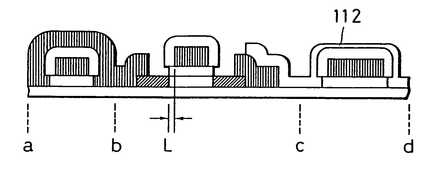
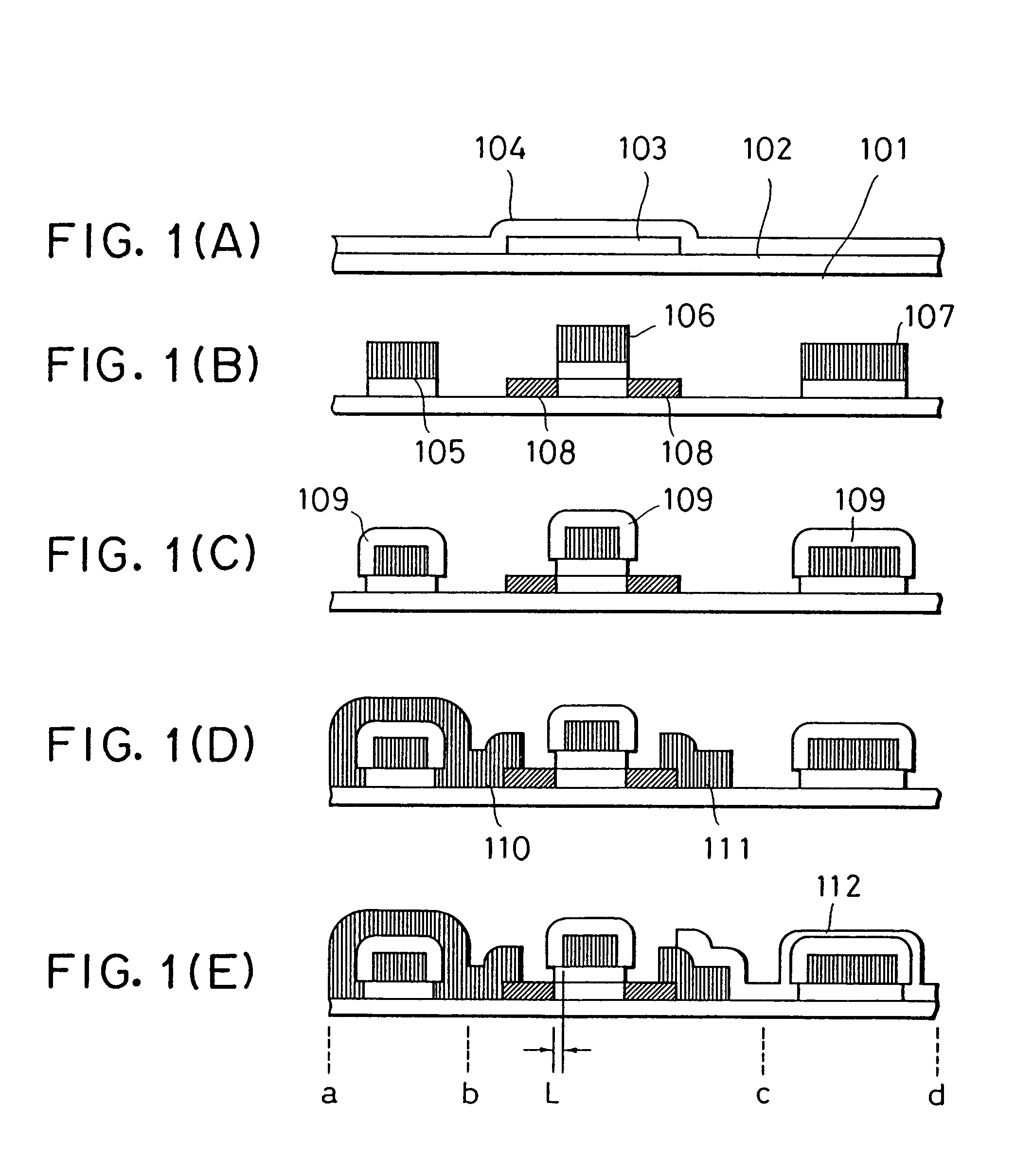
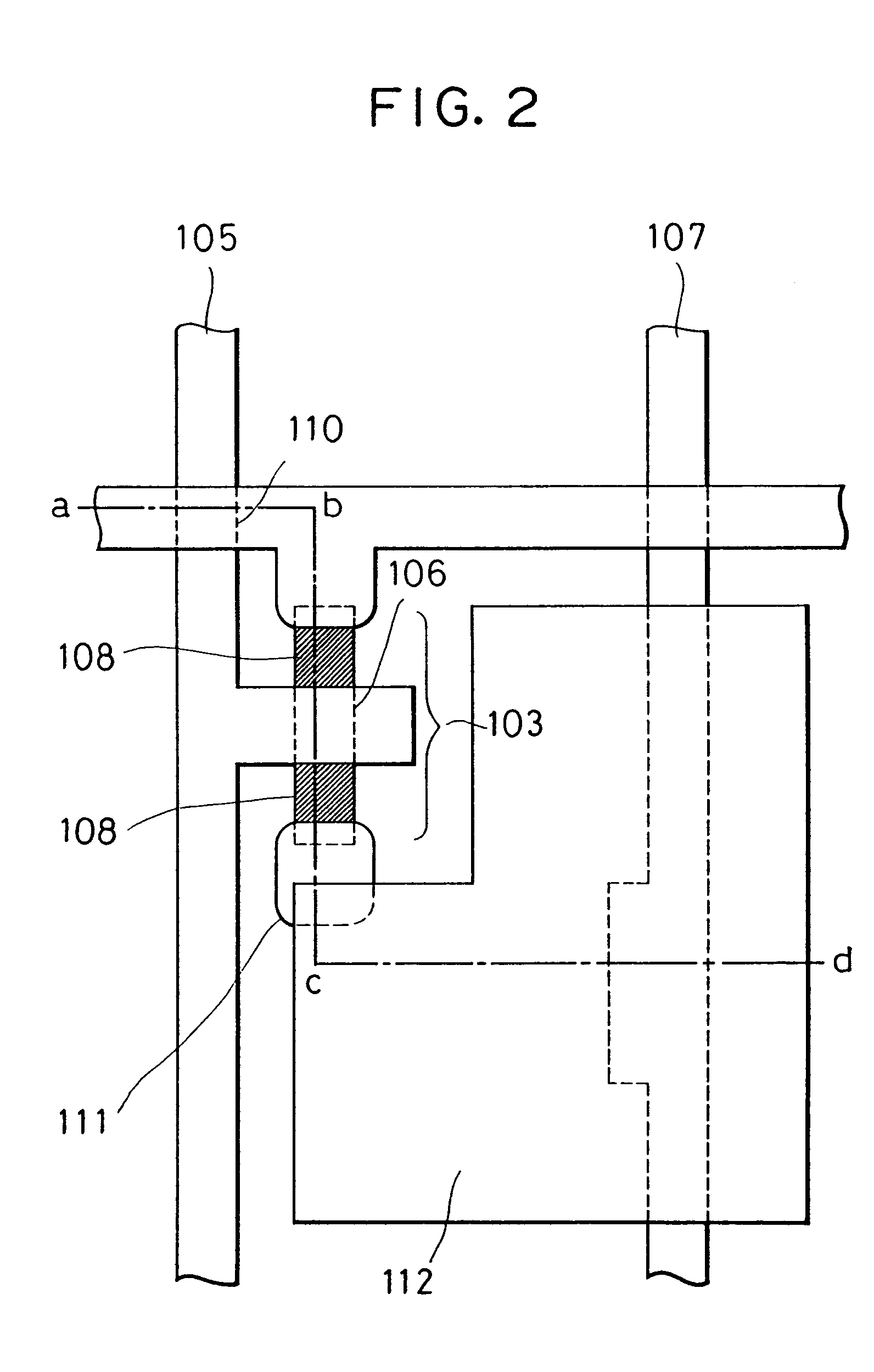
[0069]Example 1 of the present invention is now described by referring to FIG. 10. The invention is applied to CMOS TFTs fabricated on an AN glass substrate. First, as shown in FIG. 10(A), a silicon nitride film 152a was formed to a thickness of 100 nm on the AN glass substrate 151 by low-pressure CVD. Dichlorosilane (SiH2Cl2) and ammonia were used as raw material gases in the low-pressure CVD. The pressure was 10 to 1000 Pa. The temperature was 500–800° C., preferably between 550 and 750° C. Of course, silane (SiH4) or trichlorosilane (SiHCl3) may also be used. Instead of the low-pressure CVD, other CVD techniques such as plasma CVD, photo-assisted CVD, or plasma-enhanced CVD may be exploited.

[0070]The silicon nitride film formed in this way prevents the moving ions such as sodium ions contained in the glass substrate from entering the semiconductor. Therefore, if the amount of the moving ions in the substrate is sufficiently small, then it is not necessary to form the silicon nitr...


PUM


Abstract

A thin-film semiconductor device or integrated circuit comprising an insulating substrate, TFTs (thin-film transistors) formed on the substrate, and multilayer conductive interconnections. The circuit has a first metallization layer becoming gate electrodes and gate interconnections. The surface of the first metallization layer is oxidized by anodic oxidation to form an insulating coating on the surface of the first metallization layer. A second metallization layer becoming source and drain electrodes or conductive interconnections is then formed on the insulating coating directly or via an interlayer insulator. An improvement in the production yield and improved reliability are accomplished.

Description

[0001]This application is a Continuation of Ser. No. 07 / 949,135 filed Sep. 23, 1992, now abandoned.FIELD OF THE INVENTION[0002]The present invention relates to a highly reliable semiconductor device or semiconductor integrated circuit which is formed on an insulating substrate and can be mass-produced with a high production yield. The present invention also relates to a method of fabricating such a semiconductor device or integrated circuit. The invention can be applied to a circuit for driving a liquid crystal display or a thin-film image sensor and also to a three-dimensional integrated circuit.BACKGROUND OF THE INVENTION[0003]In recent years, it has been attempted to form a semiconductor integrated circuit on an insulating substrate made of a glass or sapphire, because the parasitic capacitance between the substrate and the conductive interconnections is reduced, thus improving the operating speed. Especially, where glass materials such as quartz are used, no limitations are impo...

Claims


Application Information

Patent Timeline
IPC IPC(8): H01L21/336H01L21/77H01L21/84H01L27/13
CPCH01L29/66757H01L27/1255
Inventor YAMAZAKI, SHUNPEITAKEMURA, YASUHIKOMASE, AKIRAUOCHI, HIDEKI
Owner SEMICON ENERGY LAB CO LTD
Features
  • Generate Ideas
  • Intellectual Property
  • Life Sciences
  • Materials
  • Tech Scout
  • Unparalleled Data Quality
  • Higher Quality Content
  • 60% Fewer Hallucinations
Learn More