Transmission electron microscope sample preparation

a technology of electron microscope and electron microscope, which is applied in the field of electron microscope sample preparation, can solve the problems of inability to femto-laser machining, inconvenient use, and inability to achieve the effect of reducing the cost per sample, convenient use, and convenient us

Inactive Publication Date: 2006-01-03
OXFORD INSTR AMERICA
View PDF14 Cites 43 Cited by
  • Summary
  • Abstract
  • Description
  • Claims
  • Application Information

AI Technical Summary

Benefits of technology

[0022]This invention replaces the diamond saw and cut or machine with a laser. Typical laser machining leaves thermal damage on the micrometer scale. Since the device size scale is micrometers and less, thermal damage is unacceptable. To eliminate thermal damage caused by laser ablation, a femtosecond (one quadrillionth or 10−15 second) laser is used in the present invention.
[0024]The advantage of the laser milling technology of the present invention over the present state of the art is that it does not require the removal of a fragile membrane from a silicon wafer, which is the case with current FIB TEM sample preparation. Rather, a laser removes a shaped block from the wafer which contains an area thinned for TEM and guide holes for mounting to a bracket designed to fit both FIB and TEM instruments.
[0026]The laser-milling instrument of the present invention as a whole represents an innovation, with the newest portion including the laser itself. The phenomenon of laser ablation of silicon has been studied for years, but the results with older nanosecond-regime (NR) laser technologies would not suffice for the small structures of current and near-future silicon integrated-circuit technologies. Lasers operating in the sub-picosecond regime (SPR) are relatively new inventions, and have only been applied to the ablation of silicon since about 1995. These lasers offer the promise of superior performance, and ease of application to milling.
[0027]The present invention is a new technique having a number of advantages over the current commercially available solutions. Instead of trying to extract a fragile, minuscule membrane from a wafer after FIB processing, a laser is used to cut out a uniform sample shaped block containing the thinned area of interest and a pair of laser drilled holes. The holes are mated to twin probes mounted on a bracket that can be fitted directly to a FIB stage or modified TEM holder. The membrane is protected by the bracket throughout the preparation and transfer steps of the process. Because the sample has been pre-cut with a precision laser, there is a minimum of actual trimming required in the FIB, eliminating 45 minutes to two hours of milling time.
[0030]The process of the present invention provides a safe, easy to use, semi-automated, and efficient method for cutting and extracting a specific nano-level feature from a wafer. The method allows a user to remove most of the material in situ, while also providing protection for subsequent steps. The holder or holder tip can then be placed inside a FIB for final thinning, followed by direct transfer into the TEM.
[0031]The TEM sample preparation of the present invention results in lower costs per sample. A comparison of the costs involved with TEM sample preparation using the present invention versus using other currently available methods is summarized in Table 1.

Problems solved by technology

Typical laser machining leaves thermal damage on the micrometer scale.
Since the device size scale is micrometers and less, thermal damage is unacceptable.
Femto-laser machining is not well known; however, it has been done on various materials for a couple of years.

Method used


Image

  • Transmission electron microscope sample preparation
  • Transmission electron microscope sample preparation
  • Transmission electron microscope sample preparation

Examples


Embodiment Construction

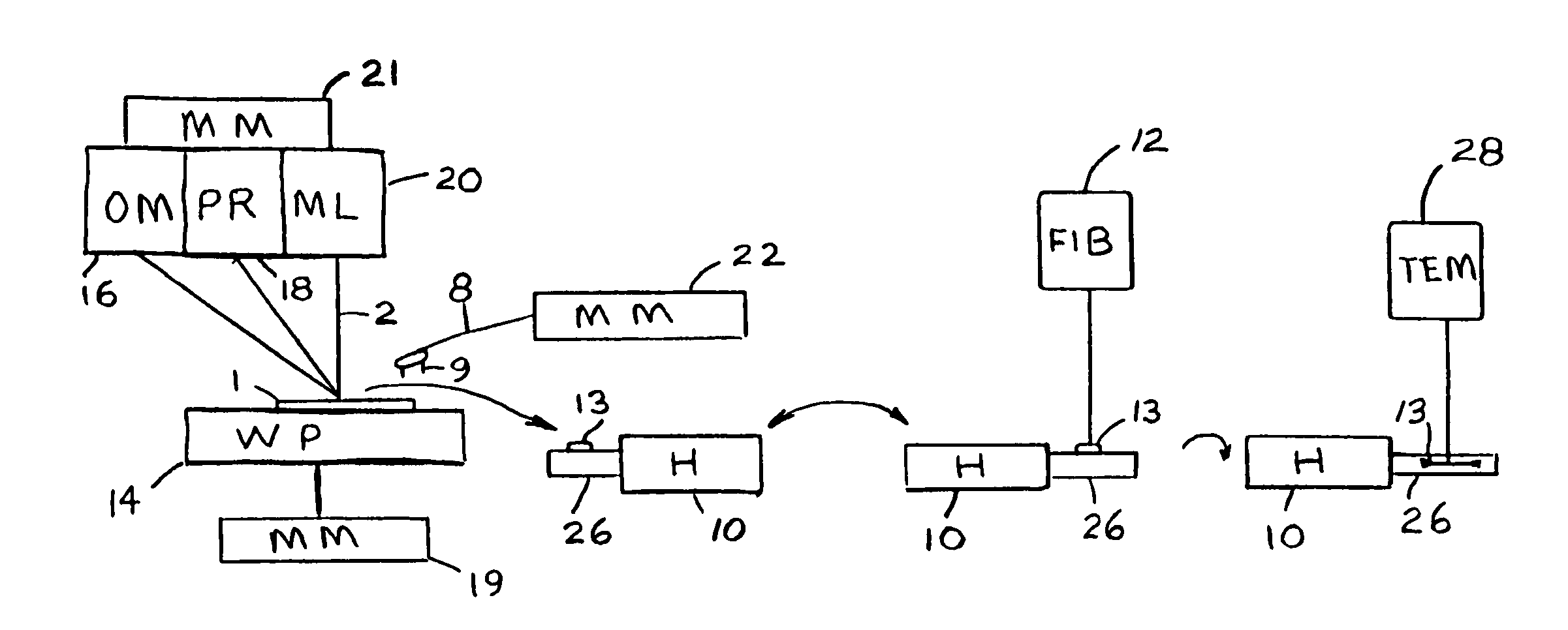
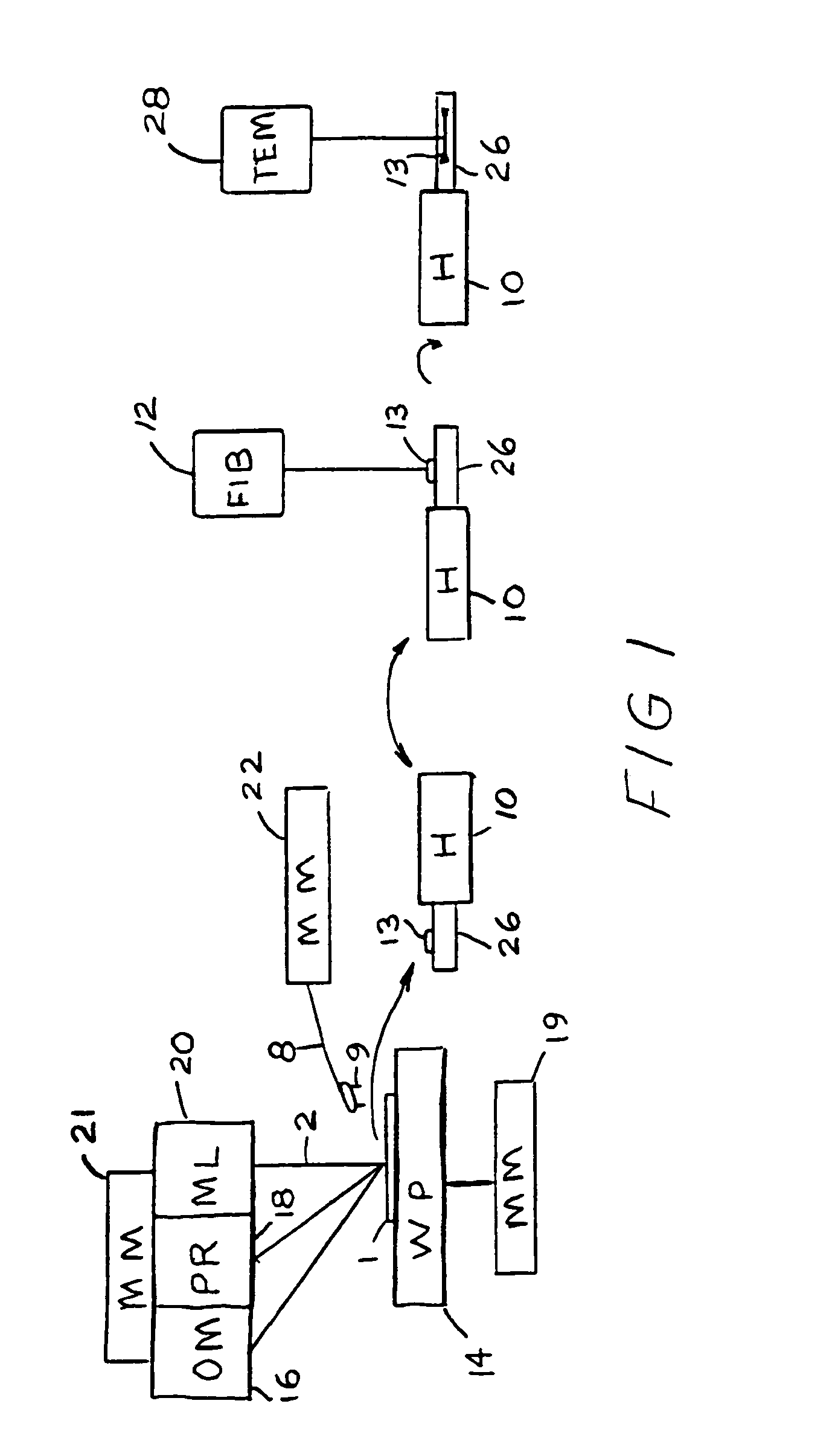
[0037]The process of the present invention provides a safe, easy to use, semi-automated, and efficient method for cutting and extracting a specific nano-level feature from a wafer. The method allows a user to remove most of the material in situ, while also providing protection for subsequent steps. The holder or holder tip can then be placed inside a FIB for final thinning, followed by direct transfer into the TEM.

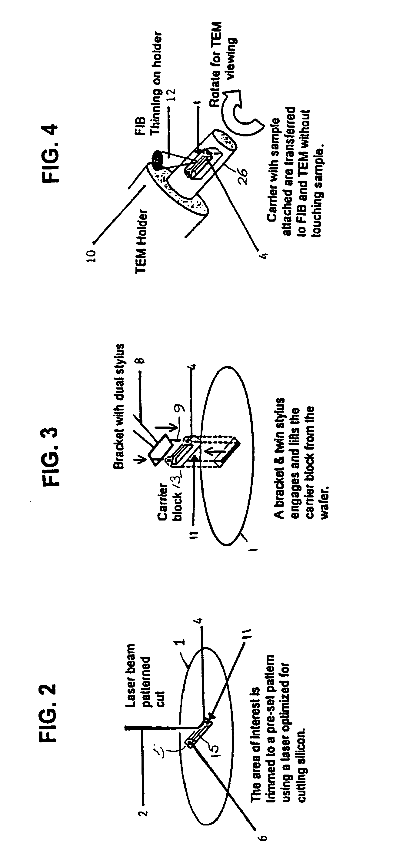
[0038]As shown in FIG. 1, a preferred embodiment of the TEM sample preparation apparatus of the present invention has a wafer stage platform 14 and an optical microscope 16. A computer operated pattern recognition assembly 18 is connected to the optical microscope for automatically addressing specific locations of areas of interest 4 on the wafer 1 as selected by the optical microscope. Preferably, a milling laser 20 is attached to the optical microscope 16 to mill a set pattern around an area of interest 4 of the wafer 1. The pattern includes forming a thin sample strip 1...


PUM

PropertyMeasurementUnit
atomic sizeaaaaaaaaaa

Abstract

Sample preparation apparatus and method includes a wafer stage platform with an optical microscope and integrated pattern recognition to automatically address specific locations on the wafer sample of interest. A laser attaches to the optical microscope to mill a set pattern around the area of interest. A precision micro-manipulator engages the sample support structure, extracts the structure, and places the structure in a TEM holder or holder tip. The holder or holder tip can then be placed inside a FIB for final thinning, followed by direct transfer into the TEM.

Description

CROSS-REFERENCE TO RELATED APPLICATION[0001]This is a continuation of U.S. patent application Ser. No. 09 / 920,715 filed Aug. 3, 2001, now U.S. Pat. No. 6,841,788.[0002]This application claims the benefit of U.S. Provisional Application No. 60 / 222,728 filed Aug. 3, 2000.BACKGROUND OF THE INVENTION[0003]Transmission electron microscopes (TEMs) have been used in a variety of scientific disciplines for 50 years. A TEM works in a way fundamentally similar to a light microscope except for the use of an electron beam instead of light. Electrons have a much shorter wavelength and consequently allow viewers to see features approaching atomic size (<1 nanometer) in comparison to a limit of 100 nm (0.1 μm for light).[0004]Over the last 50 years, transmission electron microscopy (TEM) technology and its applications have undergone tremendous advances. TEM has become an important analytical tool in many disciplines that require visualization and / or imaging of features less than one nanometer ...

Claims


Application Information

Patent Timeline
Patent Type & Authority Patents(United States)
IPC IPC(8): H01J37/31B23K26/38G01N1/32G01N23/225G21K7/00
CPCG01N1/32G01N23/225H01J2237/3174H01J2237/2817G01N2001/2886
Inventor ROBINSON, JOSEPHCHURCH, KENNETH H.
Owner OXFORD INSTR AMERICA
Why Eureka
Try Eureka