Apparatus and methods for a physical layout of simultaneously sub-accessible memory modules

a memory module and physical layout technology, applied in the field of memory modules, can solve problems such as hammering the speed at which advanced computer systems may operate, and achieve the effect of improving the performance of memory modules

Active Publication Date: 2006-01-03
MICRON TECH INC
View PDF23 Cites 157 Cited by
  • Summary
  • Abstract
  • Description
  • Claims
  • Application Information

AI Technical Summary

Benefits of technology

[0008]The present invention is directed to apparatus and methods for a physical layout for simultaneously sub-accessible memory modules for computer systems. In one aspect, a memory module includes a printed circuit board having a plurality of sectors, each sector being electrically isolated from the other sectors and having a multi-layer structure. At least one memory device is attached to each sector or rank. A driver is a

Problems solved by technology

One drawback, for example, is that because the memory interface 52 is shared between the two ranks 62, the driver chip 64 accesses only

Method used


Image

  • Apparatus and methods for a physical layout of simultaneously sub-accessible memory modules
  • Apparatus and methods for a physical layout of simultaneously sub-accessible memory modules
  • Apparatus and methods for a physical layout of simultaneously sub-accessible memory modules

Examples


Embodiment Construction

[0019]The present description is generally directed toward novel apparatus and methods for a physical layout of simultaneously sub-accessible memory modules. Many specific details of certain embodiments of the invention are set forth in the following description and in FIGS. 4–9 to provide a thorough understanding of such embodiments. One skilled in the art will understand, however, that the present invention may have additional embodiments, or that the present invention may be practiced without several of the details described in the following description.

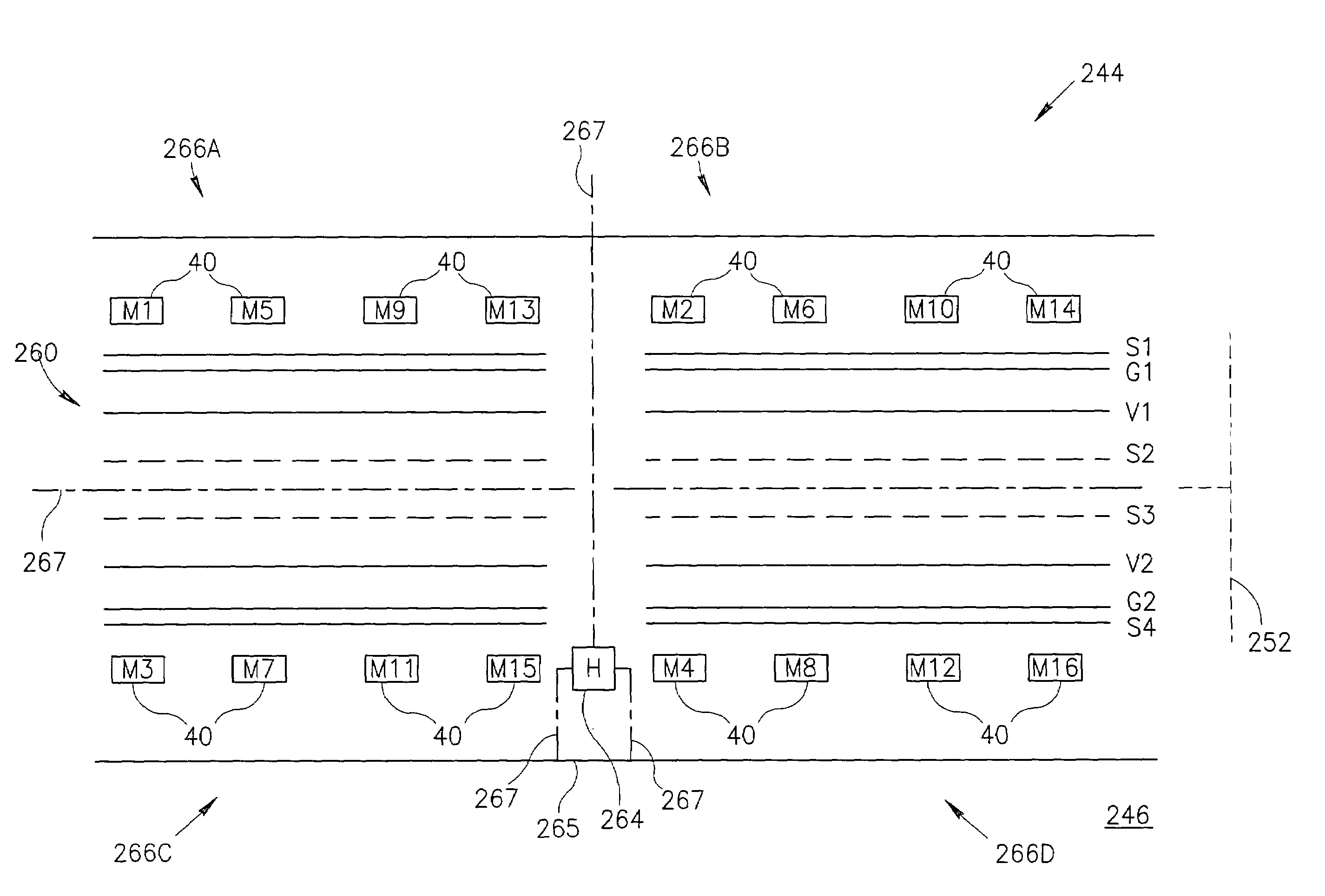
[0020]FIG. 4 is a top schematic representation of a PCB stackup 160 of a memory module 144 in accordance with an embodiment of the invention. FIG. 5 is a side elevational view of the memory module 144 of FIG. 4. In this embodiment, the memory module 144 includes four sectors 166. As shown in FIG. 4, each sector 166 includes first, second, third, and fourth signal layers S1, S2, S3, S4, first and second ground layers G1, G2, and fi...


PUM


Abstract

A layout for simultaneously sub-accessible memory modules is disclosed. In one embodiment, a memory module includes a printed circuit board having a plurality of sectors, each sector being electrically isolated from the other sectors and having a multi-layer structure. At least one memory device is attached to each sector, the memory devices being organized into a plurality of memory ranks. A driver is attached to the printed circuit board and is operatively coupled to the memory ranks. The driver is adapted to be coupled to a memory interface of the computer system. Because the sectors are electrically-isolated from adjacent sectors, the memory ranks are either individually or simultaneously, or both individually and simultaneously accessible by the driver so that one or more memory devices on a particular sector may be accessed at one time. In an alternate embodiment, the printed circuit board includes a driver sector electrically isolated from the other sectors and having a multi-layer structure, the driver being attached to the driver sector.

Description

TECHNICAL FIELD[0001]The present invention relates to memory modules, and more particularly to novel apparatus and methods for a physical layout of simultaneously sub-accessible memory modules.BACKGROUND OF THE INVENTION[0002]A conventional computer system 10 shown in FIG. 1 includes a central processing unit (“CPU”) 12, such as a microprocessor, that is coupled to a bus bridge 16, memory controller or the like. The CPU 12 is also typically coupled to a cache memory 18 to allow instructions and data to be more frequently accessed by the CPU 12. The bus bridge 16 allows the CPU 12 to receive program instructions from a system memory 20. The CPU 12 can also write data to and read data from the system memory 20 through the bus bridge 16. The CPU 12 also preferably transfers video data from the system memory 20 to a display system including a graphics processor or graphics accelerator 24, a video RAM 26, and a conventional display 28, such as a cathode ray tube (“CRT”), liquid crystal d...

Claims


Application Information

Patent Timeline
IPC IPC(8): G11C11/401H05K1/00H05K1/18
CPCG11C5/02H05K1/181H05K1/0298H05K2201/09972Y02P70/50
Inventor LEE, TERRY R.JEDDELOH, JOSEPH M.
Owner MICRON TECH INC
Why Eureka
Try Eureka