Semiconductor integrated circuit device and cellular terminal using the same

a technology of integrated circuit and cellular terminal, which is applied in the direction of semiconductor devices, semiconductor/solid-state device details, instruments, etc., can solve the problems of reducing the on-state current inhibiting high-speed operation, and reducing the power consumption of the integrated circuit, so as to prevent the unstable operation of the mos transistor circuit and the increase of current consumption. , the effect of suppressing the gate curren

Inactive Publication Date: 2006-01-10
SHARP KK
View PDF17 Cites 13 Cited by
  • Summary
  • Abstract
  • Description
  • Claims
  • Application Information

AI Technical Summary

Benefits of technology

[0018]Accordingly, the present invention provides a semiconductor integrated circuit device, as well as a portable terminal using the device, which is capable of suppressing the increase of the gate current and thereby preventing unstable operations of the MOS transistor circuit and the increase of the current consumption even in the

Problems solved by technology

These large design margins cause obstruction to downsizing or power consumption reduction of integrated circuits.
In a semiconductor integrated circuit device, since power consumption of the integrated circuit due to switching is proportional to the square of the power voltage, it is effective to lower the power voltage in terms of power consumption reduction, but there is a problem that lowering the power voltage alone would cause the ON-state current of a MOS transistor to decrease, inhibiting the high-speed operation.
However, decreasing the absolute value of the threshold voltage would give rise to another problem that the OFF-state current by a subthreshold current of the MOS transistor to increase.
From now onward, as the further micro-fining of integrated circuits as well as the reduction of power voltage adv

Method used


Image

  • Semiconductor integrated circuit device and cellular terminal using the same
  • Semiconductor integrated circuit device and cellular terminal using the same
  • Semiconductor integrated circuit device and cellular terminal using the same

Examples


Embodiment Construction

[0074]Hereinbelow, the semiconductor integrated circuit device of the present invention as well as the portable terminal using the device are described in detail by way of embodiments thereof illustrated in the accompanying drawings.

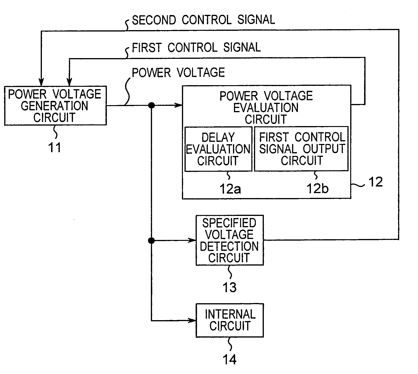
[0075]FIG. 1 is a block diagram showing the construction of a semiconductor integrated circuit device according to an embodiment of the present invention.

[0076]This semiconductor integrated circuit device, as shown in FIG. 1, has a power voltage generation circuit 11 for generating a power voltage, a power voltage evaluation circuit 12 as a first power voltage control circuit for receiving as an input a power voltage derived from the power voltage generation circuit 11 and producing as an output a first control signal to the power voltage generation circuit 11, a specified voltage detection circuit 13 as a second power voltage control circuit for receiving as an input a power voltage derived from the power voltage generation circuit 11 and producing as a...


PUM


Abstract

In a semiconductor integrated circuit device, a first control signal outputted from the power voltage evaluation circuit controls power voltage of the power voltage generation circuit so that the power voltage becomes lower within a range over which the internal circuit normally operates, while a second control signal outputted from the specified voltage detection circuit controls the power voltage of the power voltage generation circuit so that the power voltage generated by the power voltage generation circuit does not become equal to or higher than a specified voltage. This makes the power voltage as low as possible within the normally operational range of the internal circuit and suppresses increase of the gate current, so that unstable operations and current consumption increase of the MOS transistor can be prevented.

Description

TECHNICAL FIELD[0001]The present invention relates to a semiconductor integrated circuit device equipped with a power voltage generation circuit for a supplying power voltage to an internal circuit, and also to a portable terminal using the device.BACKGROUND ART[0002]Generally, for integrated circuits in which arithmetic processing or the like is performed in accordance with an operation clock, there is a need for providing large design margins in order to ensure normal operations at all times against variations in manufacturing processes or such variations as power supply variations and temperature changes. That is, in order that the processing time falls within one cycle time of the clock even if the circuit delay is increased by various types of changes or the like so that the processing time is increased, design margin are provided by constructing circuits in parallel fashion to suppress the processing time, or by applying a power voltage higher than that at which the integrated...

Claims


Application Information

Patent Timeline
IPC IPC(8): G05F1/10G05F3/24H01L21/822H01L27/04H01L27/02
CPCG05F3/24G05F3/242H01L27/0251
Inventor TOYOYAMA, SHINJI
Owner SHARP KK
Why Eureka
Try Eureka