CMOS sensor array with a memory interface

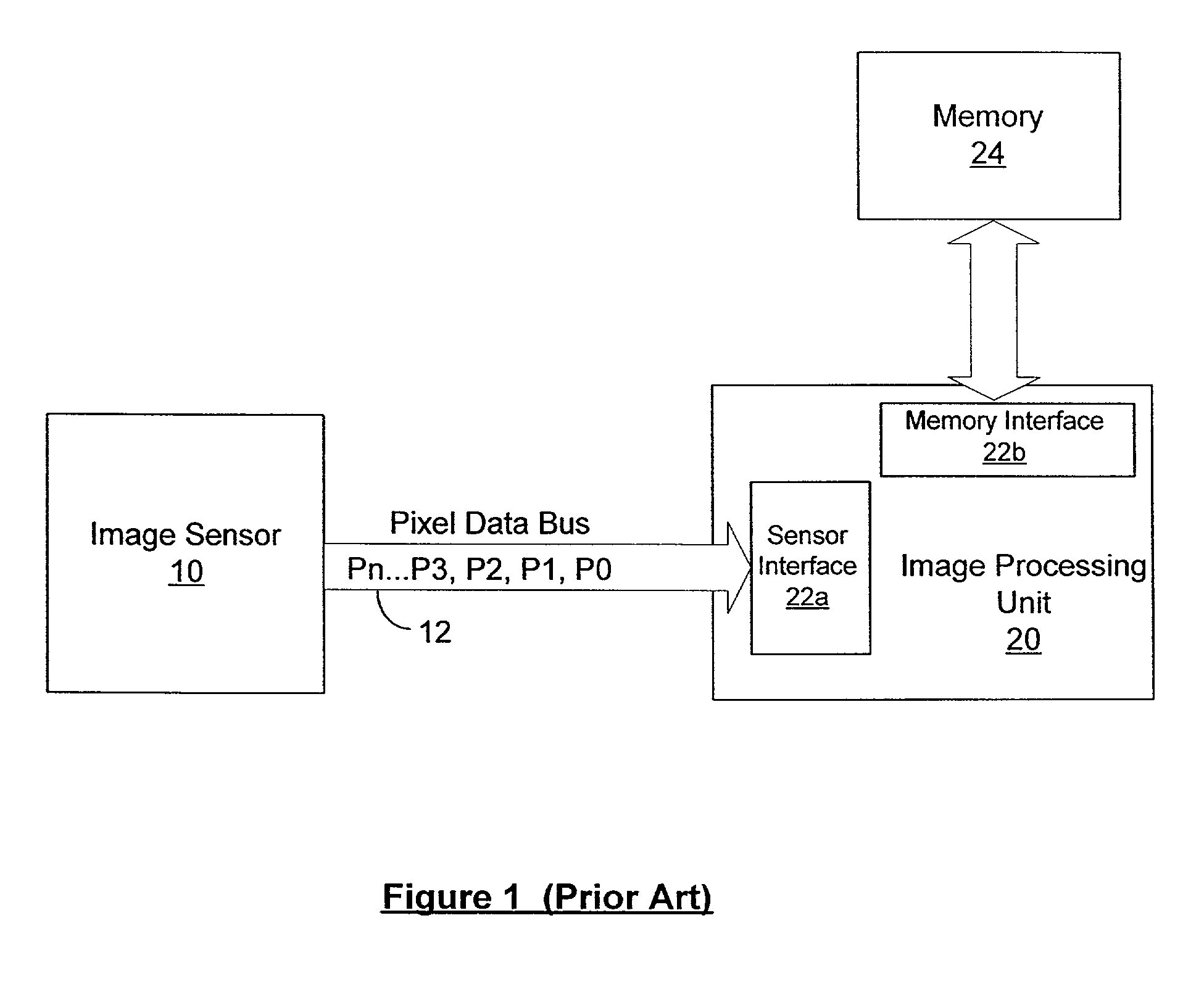
a memory interface and sensor array technology, applied in the field of image sensor systems, can solve the problems of inability to work in the way of digital cameras, inability to read out sensors at the same time, and limited speed of conventional digital imaging systems, so as to reduce the operational complexity of the image processing unit and improve efficiency.

Inactive Publication Date: 2006-01-10
PIXIM
View PDF25 Cites 43 Cited by
  • Summary
  • Abstract
  • Description
  • Claims
  • Application Information

AI Technical Summary

Benefits of technology

[0015]By including a memory interface in the image sensor of the present invention, the image sensor can be coupled directly to the memory interface port of an external image processing unit. The image processing unit is able to access the image sensor using conventional memory access protocols, thus improving the efficiency and reducing operational complexity of the image processing unit.

Problems solved by technology

Digital cameras, however, do not work in the way that traditional film cameras do.
First, because pixel data are read out one pixel at a time from the image sensor, sensor readout can be undesirably slow, particularly for large image array.
The speed of the conventional digital imaging system is limited by the pixel transmission rate of the pixel data bus 12 and the pixel data bus becomes the data transmission bottleneck of the imaging system.
Second, image sensor 10 exports pixel data according to a preloaded pixel access pattern and the access pattern cannot be changed readily during sensor readout.

Method used


Image

  • CMOS sensor array with a memory interface
  • CMOS sensor array with a memory interface
  • CMOS sensor array with a memory interface

Examples


Embodiment Construction

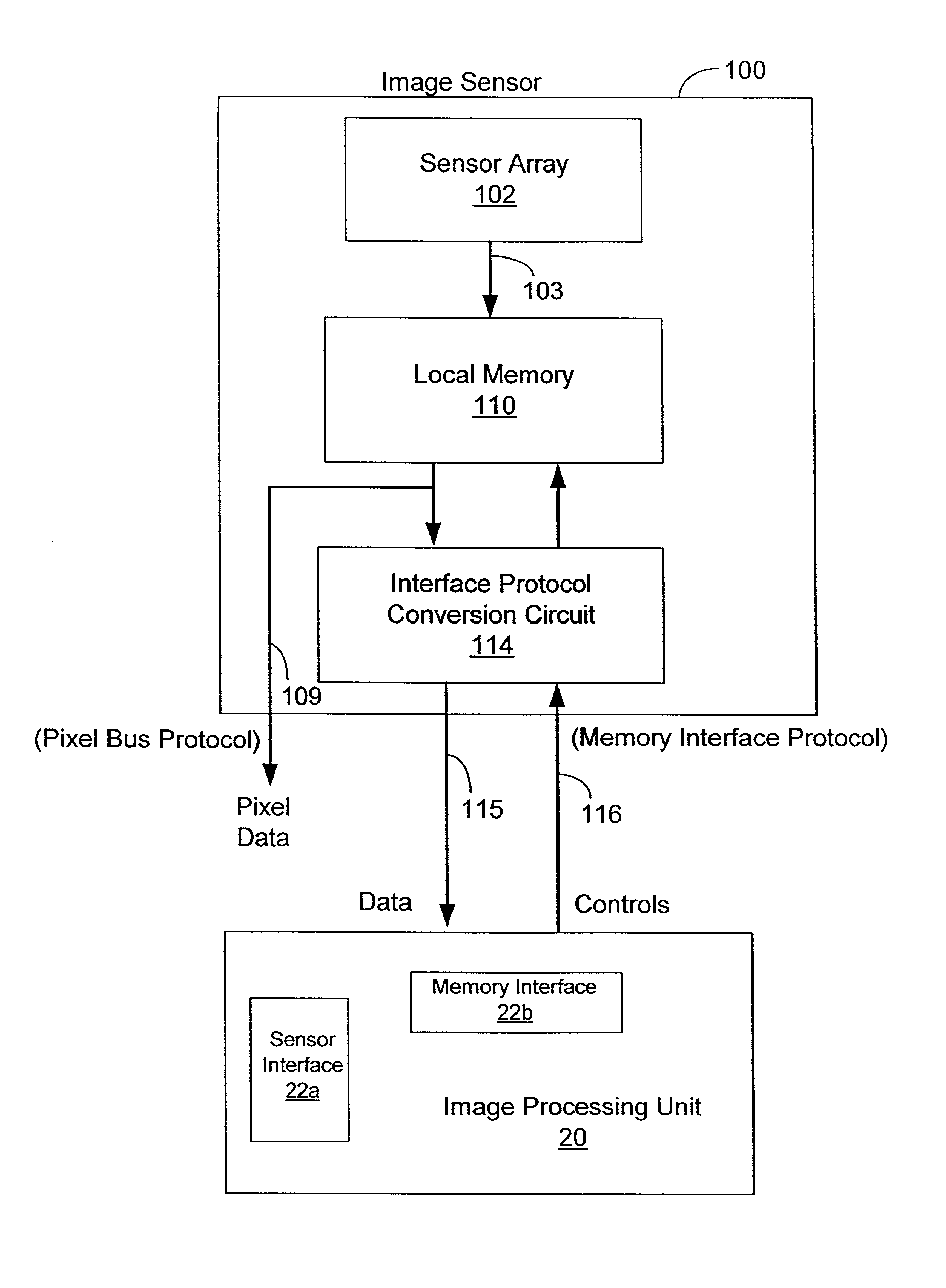
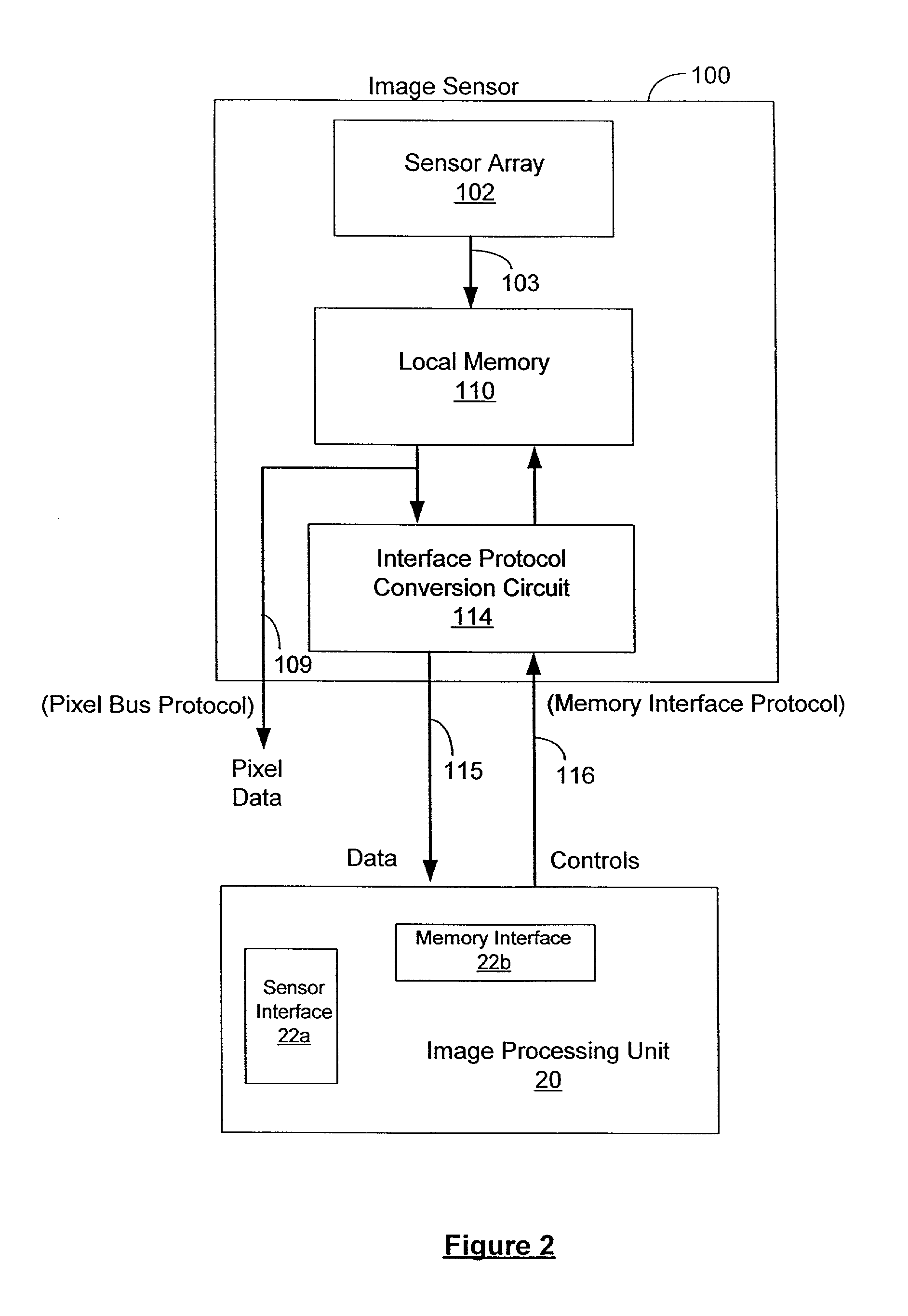
[0023]According to the present invention, an image sensor includes an integrated on-chip memory and a memory interface for outputting pixel data. By including a memory interface in the image sensor of the present invention, the image sensor can be coupled directly to the memory interface port of an external image processing unit. The image processing unit is able to access the image sensor using conventional memory access protocols. In some embodiments, an image sensor of the present invention supports a SRAM, a DRAM or a RAMBUS memory interface. By providing an on-chip memory and a memory interface in an image sensor, the image sensor of the present invention facilitates high speed pixel readout between the image sensor and the image processing device. The pixel data transmission bandwidth is limited only by the speed of the memory interface. Furthermore, by using the memory interface of the image sensor for sensor readout, the image processing device can access pixel data in the i...


PUM


Abstract

An image sensor includes a sensor or a pixel array, a data memory, and a logic circuit, all fabricated on the same integrated chip. The sensor or pixel array outputs digital signals as pixel data representing an image of a scene. The data memory is coupled to the sensor or pixel array for storing the pixel data. The logic circuit is coupled to the data memory and provides a memory interface for exporting the pixel data. The memory interface can be one of a SRAM, a DRAM or a packet protocol synchronous DRAM interface. Including a memory interface in the image sensor allows the image sensor to be coupled directly to the memory interface port of an external image processing unit. The image processing unit can access the image sensor using conventional memory access protocols, thus improving the efficiency and reducing the operational complexity of the image processing unit.

Description

CROSS-REFERENCE TO RELATED APPLICATION[0001]This is a continuation-in-part of U.S. application No.: 09 / 567,638, entitled “Integrated Digital Pixel Sensor Having a Sensing Area and a Digital Memory Area,” filed on May 9, 2000, now abandoned and by David Yang, et al., two of which are the co-inventor thereof.BACKGROUND OF THE INVENTION[0002]1. Field of the Invention[0003]The invention generally relates to image sensor systems; and in particular, the present invention relates to an image sensor including a memory interface.[0004]2. Background of the Invention[0005]Digital photography is one of the most exciting technologies that have emerged in the past years. With the appropriate hardware and software (and a little knowledge), anyone can put the principles of digital photography to work. Digital cameras, for example, are on the cutting edge of digital photography. Recent product introductions, technological advancements, and price cuts, along with the emergence of email and the World ...

Claims


Application Information

Patent Timeline
Patent Type & Authority Patents(United States)
IPC IPC(8): H04N3/14H01L27/146G06F12/00G06T1/00G06T1/60H04N1/00H04N1/028H04N5/232H04N5/335H04N7/14
CPCH04N1/00307H04N3/155H04N5/335H04N7/142H04N5/232H04N2201/0068H04N23/665H04N25/76H04N23/60H04N25/00
Inventor EWEDEMI, ODUTOLA OLUSEYEDENG, ZHONGHAN JOHNMOTTA, RICARDO JANSSONYANG, DAVID XIAO DONG
Owner PIXIM
Why Eureka
Try Eureka