Low selectivity deposition methods

a deposition method and low selectivity technology, applied in chemical vapor deposition coatings, coatings, capacitors, etc., can solve the problems of limited application of ald and the inability to achieve the theoretically expected quality of ald layers, and achieve the effect of slow rate and low selectivity

Inactive Publication Date: 2006-01-17
MICRON TECH INC
View PDF57 Cites 9 Cited by
  • Summary
  • Abstract
  • Description
  • Claims
  • Application Information

AI Technical Summary

Benefits of technology

[0013]In another aspect of the invention, a low selectivity deposition method includes forming a first part of a nucleation layer on a first surface of a substrate and forming a second part of a nucleation layer on a second surface of a substrate. A deposition layer may then be formed on the first and second parts of the nucleation layer substantially non-selectively on the first part of the nucleation layer compared to the second part. Substantially non-selective deposition occurs even though the first and second surfaces of the substrate exhibit a property of the deposition layer forming less readily on the first surface compared to the second surface. The deposition layer may comprise a monolayer of a first chemisorbed specie. The deposition layer may be formed by chemical vapor deposition or atomic layer deposition. The first and second part of the nucleation layer may be formed simultaneously. Also, the nucleation layer may form substantially non-selectively on the first surface of the substrate compared to the second surface. Further, a thickness of the first part of the nucleation layer may be greater than 50% of a thickness of the second part, or even greater than 80% of the thickness of the second part. The first surface of the substrate may exhibit a property of chemisorbing the first specie at a slower rate compared to the second surface.

Problems solved by technology

Even so, it is equally recognized that ALD can have limited application.
In some circumstances, the theoretically expected quality of an ALD layer is not achieved.

Method used


Image

  • Low selectivity deposition methods
  • Low selectivity deposition methods
  • Low selectivity deposition methods

Examples


Embodiment Construction

[0017]This disclosure of the invention is submitted in furtherance of the constitutional purposes of the U.S. Patent Laws “to promote the progress of science and useful arts” (Article 1, Section 8).

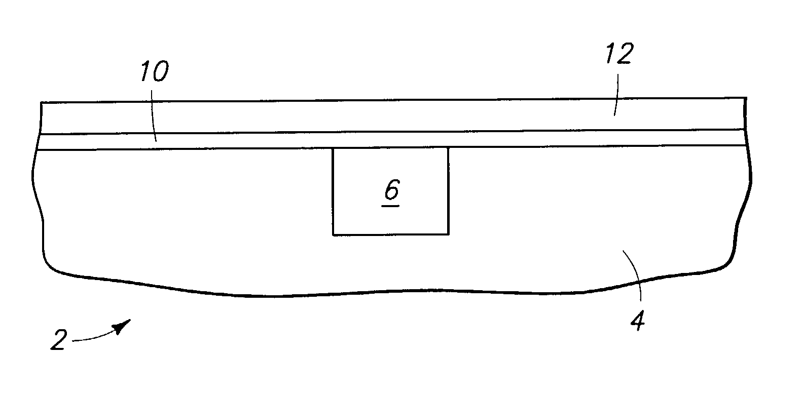
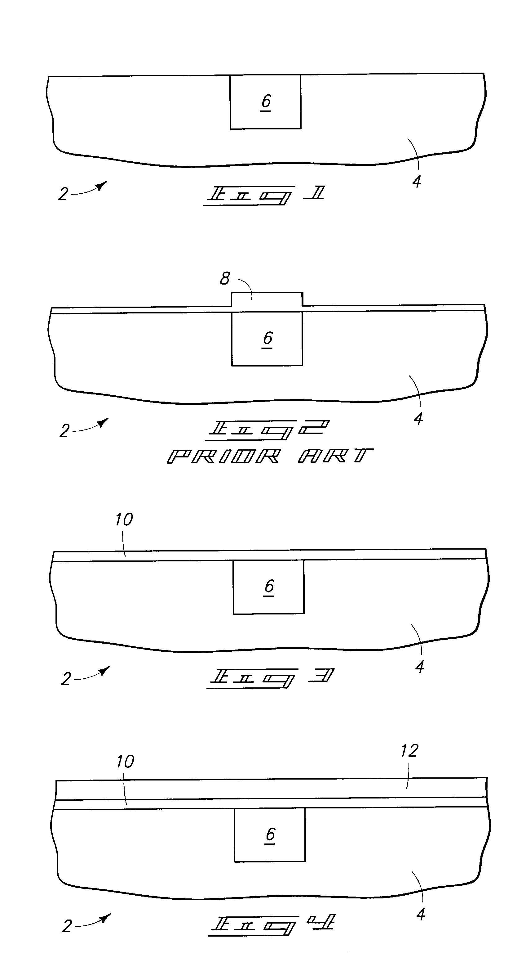
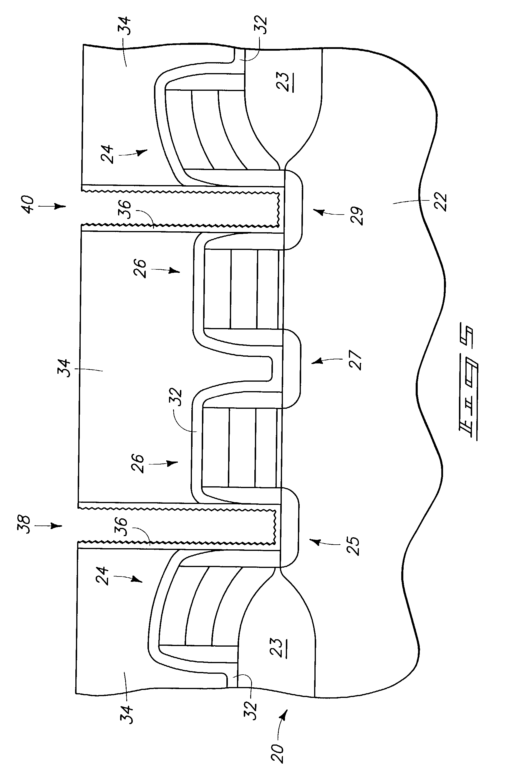
[0018]Atomic layer deposition (ALD) involves formation of successive atomic layers on a substrate. Such layers may comprise an epitaxial, polycrystalline, amorphous, etc. material. ALD may also be referred to as atomic layer epitaxy, atomic layer processing, etc. Further, the invention may encompass other deposition methods not traditionally referred to as ALD, for example, chemical vapor deposition (CVD), but nevertheless including the method steps described herein. The deposition methods herein may be described in the context of formation on a semiconductor wafer. However, the invention encompasses deposition on a variety of substrates besides semiconductor substrates.

[0019]In the context of this document, the term “semiconductor substrate” or “semiconductive substrate” is defined to me...


PUM

PropertyMeasurementUnit
thicknessaaaaaaaaaa
thicknessaaaaaaaaaa
thicknessaaaaaaaaaa

Abstract

A deposition method includes forming a nucleation layer over a substrate, forming a layer of a first substance at least one monolayer thick chemisorbed on the nucleation layer, and forming a layer of a second substance at least one monolayer thick chemisorbed on the first substance. The chemisorption product of the first and second substance may include silicon and nitrogen. The nucleation layer may comprise silicon nitride. Further, a deposition method may include forming a first part of a nucleation layer on a first surface of a substrate and forming a second part of a nucleation layer on a second surface of the substrate. A deposition layer may be formed on the first and second parts of the nucleation layer substantially non-selectively on the first part of the nucleation layer compared to the second part. The first surface may be a surface of a borophosphosilicate glass layer. The second surface may be a surface of a rugged polysilicon layer. The first and second part of the nucleation layer may be formed simultaneously.

Description

RELATED PATEN DATA[0001]This patent resulted from a divisional application U.S. patent application Ser. No. 09 / 643,004, filed on Aug. 21, 2000.TECHNICAL FIELD[0002]This invention relates to methods of atomic layer deposition and methods of low selectivity chemical vapor deposition.BACKGROUND OF THE INVENTION[0003]Atomic layer deposition (ALD) is recognized as a deposition technique that forms high quality materials with minimal defects and tight statistical process control. Even so, it is equally recognized that ALD can have limited application. In some circumstances, the theoretically expected quality of an ALD layer is not achieved.[0004]It can be seen that a need exists for an ALD method that forms a layer without introducing intolerable defects into the material.BRIEF DESCRIPTION OF THE DRAWINGS[0005]Preferred embodiments of the invention are described below with reference to the following accompanying drawings.[0006]FIG. 1 shows a cross-sectional fragmentary view of a depositio...

Claims


Application Information

Patent Timeline
Patent Type & Authority Patents(United States)
IPC IPC(8): H01L21/31C23C16/02C23C16/44C23C16/455H01L21/02H01L21/318
CPCC23C16/0272C23C16/45525H01L21/3185H01L28/91H01L28/84H01L21/02183H01L21/02178H01L21/02271H01L21/0228H01L21/0217
Inventor MERCALDI, GARRY A.
Owner MICRON TECH INC
Why Eureka
Try Eureka