Integrated circuit packages with reduced stress on die and associated substrates, assemblies, and systems

a technology of integrated circuits and substrates, applied in the field of electronic packaging, can solve the problems of reducing yield and reliability to unacceptable levels, and reducing structural strength of dielectric materials

Inactive Publication Date: 2006-01-24
INTEL CORP
View PDF4 Cites 27 Cited by
  • Summary
  • Abstract
  • Description
  • Claims
  • Application Information

AI Technical Summary

Problems solved by technology

Such dielectric materials may be structurally relatively weak and may have relatively low fracture toughness.
In known IC packages in which the contacts of a die having one or more low-K dielectric layers are electrically and mechanically coupled to corresponding lands of an IC substrate, the yield and reliability may diminish to unacceptable levels.

Method used


Image

  • Integrated circuit packages with reduced stress on die and associated substrates, assemblies, and systems
  • Integrated circuit packages with reduced stress on die and associated substrates, assemblies, and systems
  • Integrated circuit packages with reduced stress on die and associated substrates, assemblies, and systems

Examples


Embodiment Construction

[0017]In the following detailed description of embodiments of the subject matter, reference is made to the accompanying drawings, which form a part hereof, and in which is shown by way of illustration specific preferred embodiments in which the subject matter may be practiced. These embodiments are described in sufficient detail to enable those skilled in the art to practice the subject matter, and it is to be understood that other embodiments may be utilized and that structural, mechanical, compositional, electrical, and procedural changes may be made without departing from the spirit and scope of the subject matter. The following detailed description is, therefore, not to be taken in a limiting sense, and the scope of the subject matter is defined only by the appended claims.

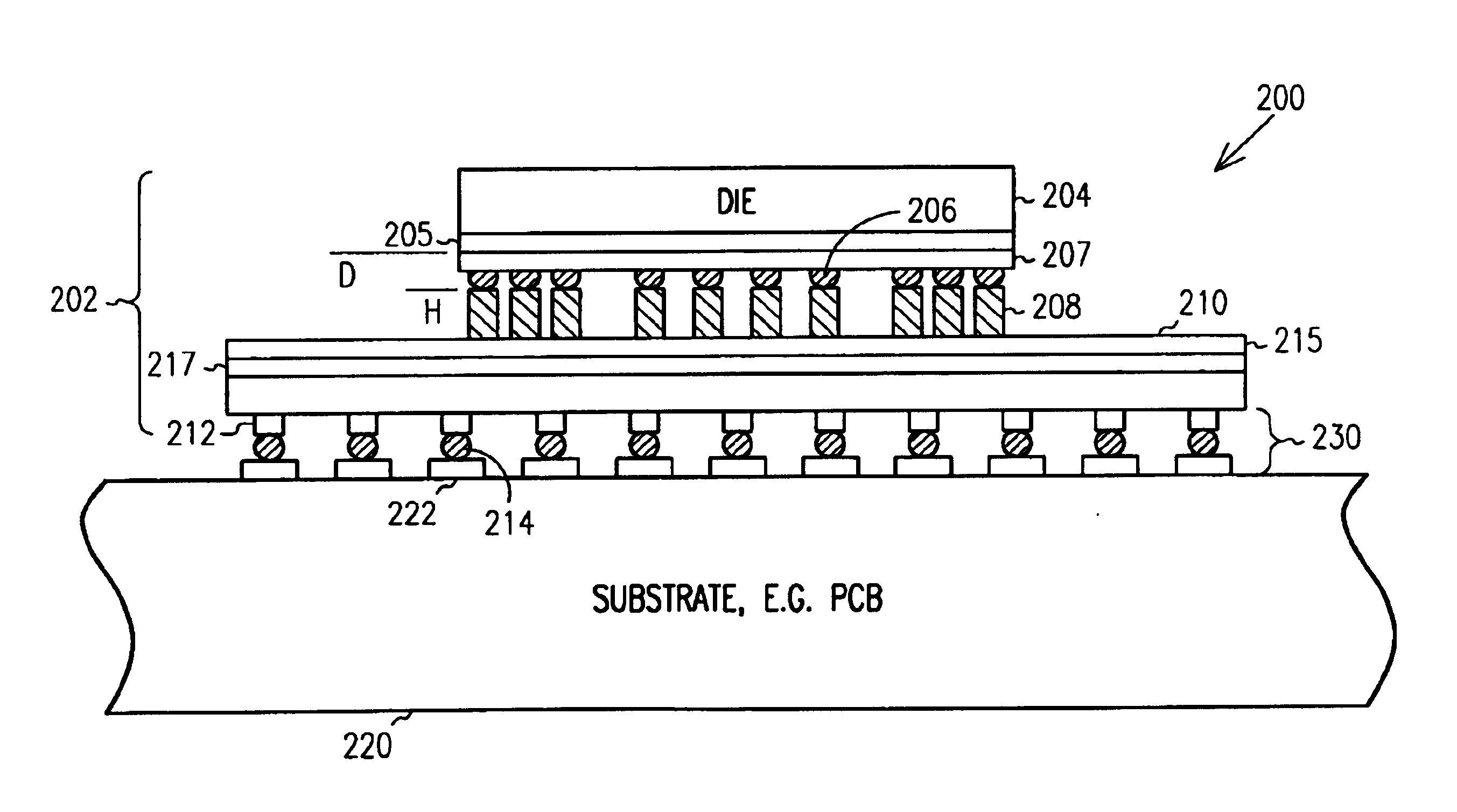
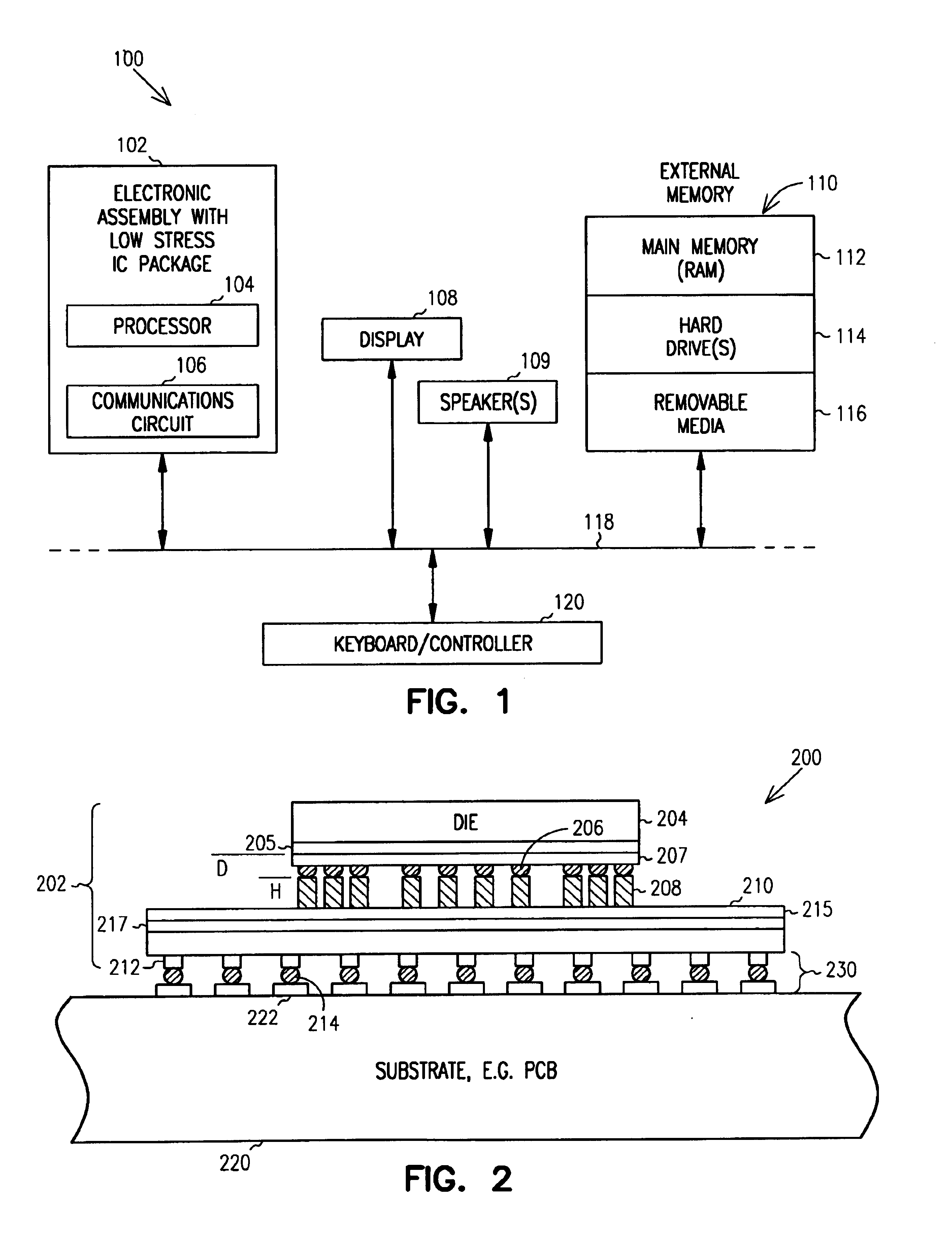
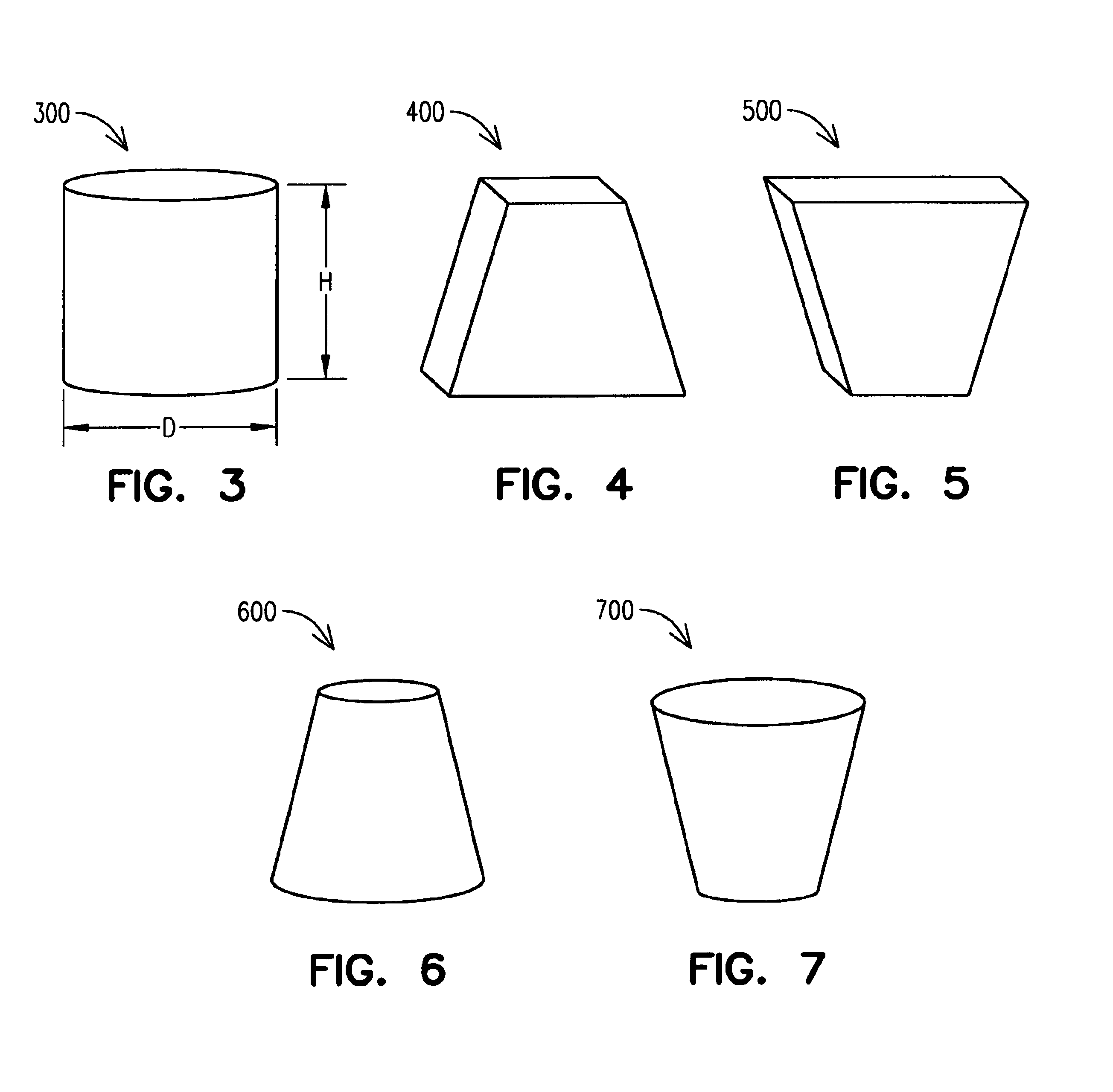
[0018]The subject matter provides a solution to certain mechanical stress problems that are associated with prior art packaging of integrated circuits. In an embodiment, the component is a die having mounting ...


PUM

PropertyMeasurementUnit
melting temperatureaaaaaaaaaa
aspect ratioaaaaaaaaaa

Abstract

Mechanical stresses are reduced between an electronic component having relatively low fracture toughness and a substrate having relatively greater fracture toughness. In an embodiment, the component may be a die having mounting contacts formed of a low yield strength material, such as solder. A package substrate has columnar lands formed of a relatively higher yield strength material, such as copper, having a relatively higher melting point than the component contacts and having a relatively high current-carrying capacity. The component contacts may be hemispherical in shape. The lands may be substantially cylinders, truncated cones or pyramids, inverted truncated cones or pyramids, or other columnar shapes. Methods of fabrication, as well as application of the package to an electronic assembly and to an electronic system, are also described.

Description

TECHNICAL FIELD[0001]The subject matter relates generally to electronics packaging and, more particularly, to an electronics package with reduced mechanical stresses between a component and a substrate on which the component is mounted, and to manufacturing methods related thereto.BACKGROUND INFORMATION[0002]An integrated circuit (“IC”) die may be assembled into an IC package by physically and electrically coupling it to a substrate made of organic or ceramic material. One or more IC packages may be physically and electrically coupled to a printed circuit board (“PCB”) to form an “electronic assembly”. The “electronic assembly” may be part of an “electronic system”. An “electronic system” is broadly defined herein as any product comprising an “electronic assembly”. Examples of electronic systems include computers (e.g., server, router, desktop, laptop, hand-held, Web appliance, etc.), wireless communications devices (e.g., cellular phone, cordless phone, pager, etc.), computer-relat...

Claims


Application Information

Patent Timeline
Patent Type & Authority Patents(United States)
IPC IPC(8): H01L23/02H01L21/60H01L23/485H01L23/498H05K1/11H05K3/34H05K3/40
CPCH01L23/49811H01L24/10H01L24/13H01L24/81H05K1/111H01L2224/13017H01L2224/13014H01L2224/13099H01L2224/81193H01L2224/8121H01L2224/81815H01L2924/01027H01L2924/01029H01L2924/0103H01L2924/01049H01L2924/01051H01L2924/01078H01L2924/01079H01L2924/01082H01L2924/01322H01L2924/14H01L2924/1433H01L2924/15311H01L2924/30105H05K3/3436H05K3/4007H05K2201/0367H05K2201/10674H01L2224/13109H01L2924/01005H01L2924/01006H01L2924/01019H01L2924/01033H01L2924/01047H01L2924/0105H01L2924/014H01L2224/16225H01L2924/00014H01L2924/00H01L2224/05001H01L2224/05023H01L2224/05568H01L2224/13Y02P70/50H01L2224/05599H01L2224/05099
Inventor AGRAHARAM, SAIRAMHANNA, CARLTONATLURI, VASUDEVAHE, DONGMING
Owner INTEL CORP
Why Eureka
Try Eureka