Semiconductor manufacturing resolution enhancement system and method for simultaneously patterning different feature types

a technology of semiconductors and manufacturing resolution, applied in the field of photolithography, can solve the problems of eluded skilled in the art for a long time, and the optical distortion becomes extremely high, and achieve the effect of reducing manufacturing time and cost and improving quality

Inactive Publication Date: 2006-02-07
CYPRESS SEMICON CORP
View PDF13 Cites 226 Cited by
  • Summary
  • Abstract
  • Description
  • Claims
  • Application Information

AI Technical Summary

Benefits of technology

[0010]The present invention provides for a method of making a mask with a transparent substrate. A first resolution enhancement structure is formed on a first portion of the transparent substrate. A second resolution enhancement structure is formed on a second portion of the tra

Problems solved by technology

As the size and density of features start to be below the wavelength of the light used to pattern the images, a different class of masks is necessary because the light is subject to diffraction and interference effects.
This is a problem when the openings are used to pattern features having sizes below the wavelength of the light used and near the resolution limit of the light.
Optical distortion becomes extremely high a

Method used


Image

  • Semiconductor manufacturing resolution enhancement system and method for simultaneously patterning different feature types
  • Semiconductor manufacturing resolution enhancement system and method for simultaneously patterning different feature types

Examples


Embodiment Construction

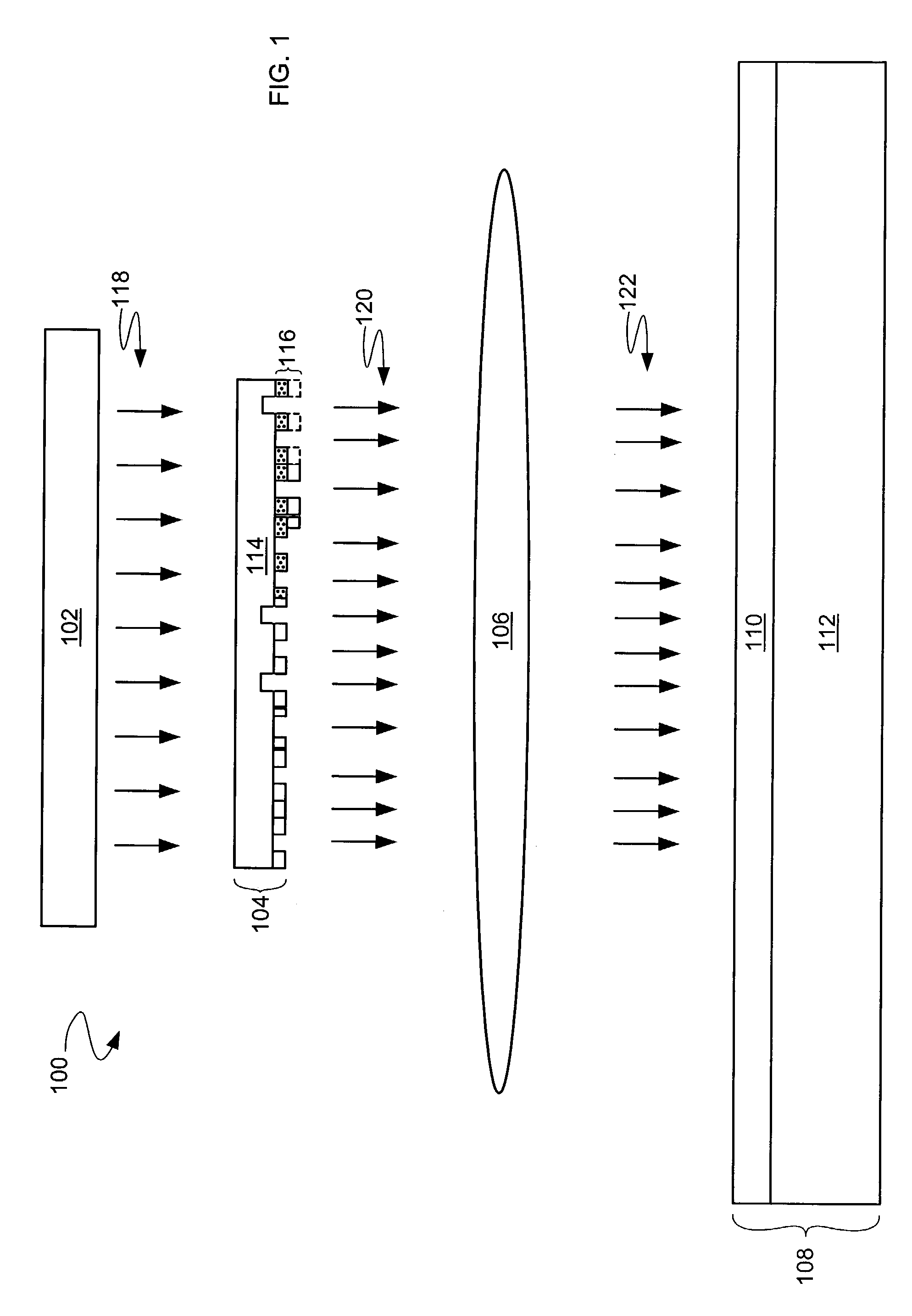
[0014]Referring now to FIG. 1, therein is shown a simplified schematic of a photolithographic system 100 using the present invention. In the photolithographic system 100, radiation is directed from an illumination source 102 through a patterned mask 104 and a lens 106 onto a semiconductor wafer 108.

[0015]The semiconductor wafer 108 includes a photoresist layer 110 on a semiconductor substrate 112, which will form a plurality of integrated circuits when completed.

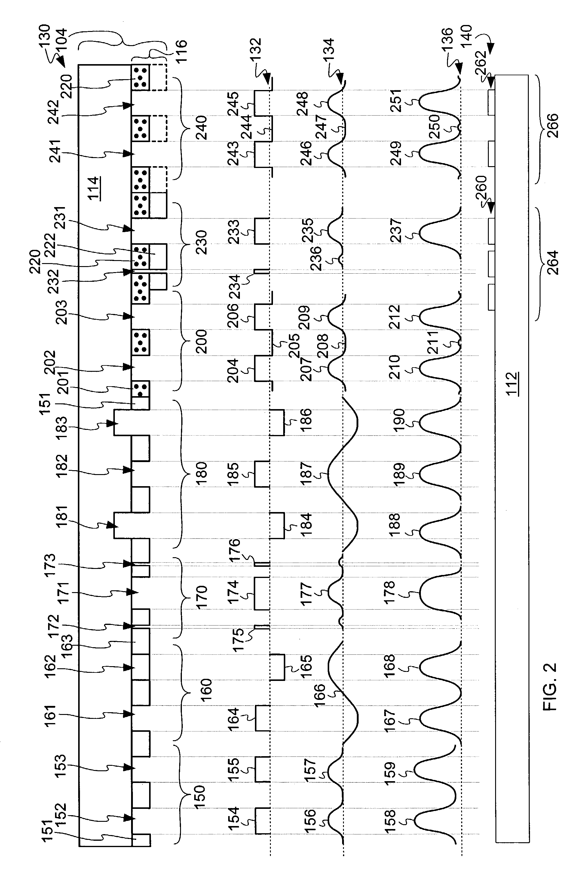
[0016]The patterned mask 104 includes a light-transparent substrate 114, of a material such as fused silica or quartz, with a patterned mask coating 116.

[0017]The term “horizontal” as used in this application is defined as a plane parallel to the conventional plane or surface of the light-transparent substrate 114, where the patterned mask coating 116 is deposited, regardless of the orientation of the substrate. The term “vertical” refers to a direction perpendicular to the horizontal as just defined. Prepositions, such as “...


PUM


Abstract

A method and system of making a mask with a transparent substrate thereon is provided. A first resolution enhancement structure is formed on the first portion of the transparent substrate. A second resolution enhancement structure is formed on a second portion of the transparent substrate, with the second resolution enhancement structure different from the first resolution enhancement structure.

Description

BACKGROUND[0001]1. Technical Field[0002]The present invention relates generally to photolithography and more particularly to patterning different types of features.[0003]2. Background Art[0004]Integrated circuits are now used in almost every type of electronic product ranging from toys to massive computers. These integrated circuits are all generally made by a photolithographic process, which involves manufacturing a template containing patterns of the electrical circuit as transparent and opaque areas. The patterned template is referred to as a “reticle” or “mask”.[0005]A radiation source, such as a light, is used to copy or “pattern” multiple images of the mask onto a photosensitive material or photoresist on the surface of a silicon wafer. Once features are patterned on the photoresist, further processing is performed to form various structures on the silicon wafer, which is subsequently cut up to form the integrated circuits. In addition to repeatedly “patterning” features onto ...

Claims


Application Information

Patent Timeline
IPC IPC(8): G03F9/00
CPCG03F1/14G03F1/0061G03F1/32G03F1/30G03F1/144G03F1/29
Inventor GHANDEHARI, KOUROSYANG, JEAN Y.SPENCE, CHRISTOPHER A.
Owner CYPRESS SEMICON CORP
Why Eureka
Try Eureka