Semiconductor device

a technology of semiconductor devices and semiconductors, applied in the field of semiconductor devices, can solve the problems of interface traps in a region, reduced channel conductance of insulated-gate sic devices, and many problems to be overcome, so as to achieve the effect of increasing the mobility of current flowing

Inactive Publication Date: 2006-02-07
PANASONIC CORP
View PDF12 Cites 113 Cited by
  • Summary
  • Abstract
  • Description
  • Claims
  • Application Information

AI Technical Summary

Benefits of technology

[0008]It is therefore an object of the present invention to take measures to effectively increase mobility of current flowing in a channel region in an accumulat

Problems solved by technology

Nevertheless, a thermal oxide film, as a gate insulating film, formed on an SiC layer has many problems remaining to be overcome.
For example, defects in a thermal oxide film cause high-density interface traps to be present in a region of the SiC layer in the vicinity of the interface with the insulating film, which have a profound effect on the electron-transport mechanism in the MIS channel.
Specifically, the interface traps existing in the region of the SiC layer in the vicinity of the interface with the insulating film cause significantly reduced channel conductance in the insulated-gate SiC device.
However, the mechanism in which defects in a thermal oxi

Method used


Image

  • Semiconductor device
  • Semiconductor device
  • Semiconductor device

Examples


first embodiment

[0062

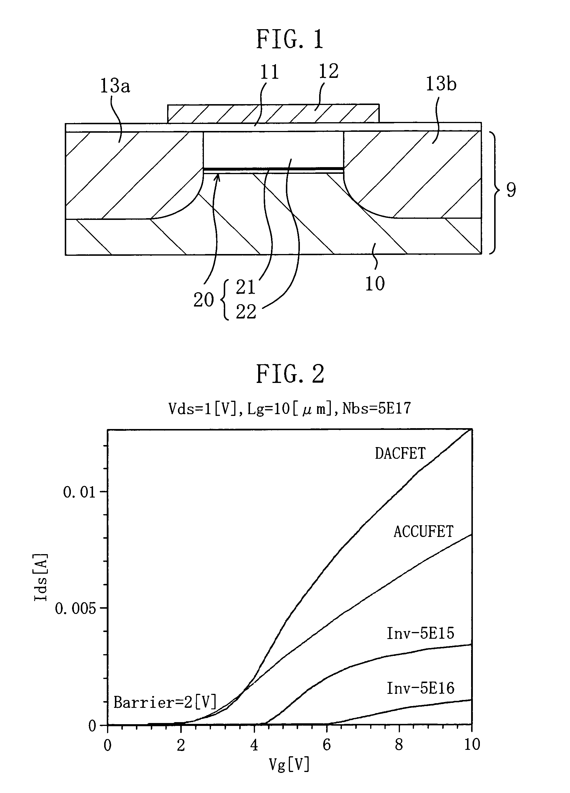
[0063]FIG. 1 is a cross sectional view illustrating the basic structure of a semiconductor device (SiC-MISFET (d-DACFET)) in accordance with a first embodiment of the present invention.

[0064]As shown in FIG. 1, the SiC-MISFET of this embodiment includes an epitaxial SiC layer 9 formed by epitaxial growth on an SiC substrate (not shown) having a 4H—SiC structure. The epitaxial SiC layer 9 includes a p-type SiC layer 10, an n-type channel layer 20, a gate insulating film 11, a gate electrode 12, an n-type source layer 13a, and an n-type drain layer 13b. The p-type SiC layer 10 is a base region. The n-type channel layer 20 is formed on the p-type SiC layer 10 and modulation-doped by in-situ doping. The gate insulating film 11 is formed on the channel layer 20 by thermal oxidation. The gate electrode 12 is formed on the gate insulating film 11. The respective n-type source and drain layers 13a and 13b are formed by implanting an n-type impurity into regions in the channel layer 20 ...

second embodiment

[0090

[0091]FIG. 7 is a cross sectional view illustrating the basic structure of a semiconductor device (SiC-MISFET (d-DACFET)) in accordance with a second embodiment of the present invention.

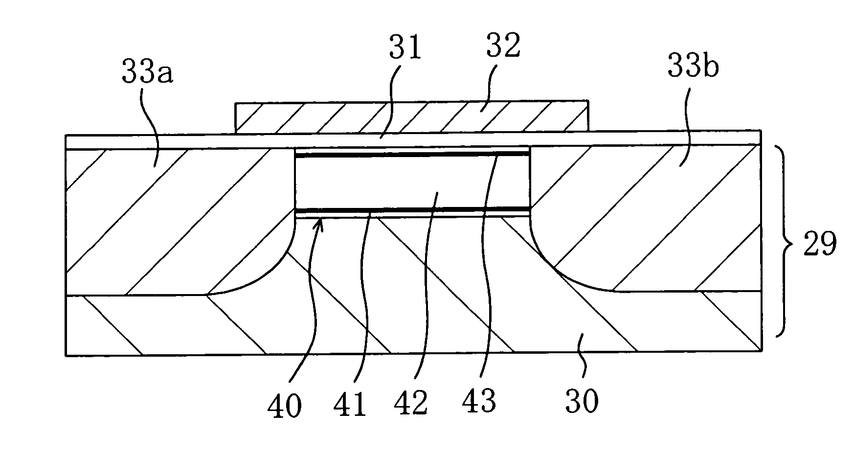
[0092]As shown in FIG. 7, the d-DACFET of this embodiment includes an epitaxial SiC layer 29 formed by epitaxial growth on an SiC substrate (not shown) having a 4H—SiC structure. The epitaxial SiC layer 29 includes a p-type SiC layer 30, which is a base region, and an n-type channel layer 40, which is formed on the p-type SiC layer 30 and modulation-doped by in-situ doping. The d-DACFET of this embodiment further includes a gate insulating film 31, a gate electrode 32, an n-type source layer 33a, and an n-type drain layer 33b. The gate insulating film 31 is formed on the channel layer 40 by thermal oxidation. The gate electrode 32 is formed on the gate insulating film 31. The respective n-type source and drain layers 33a and 33b are formed by implanting an n-type impurity into regions in the cha...

third embodiment

[0098

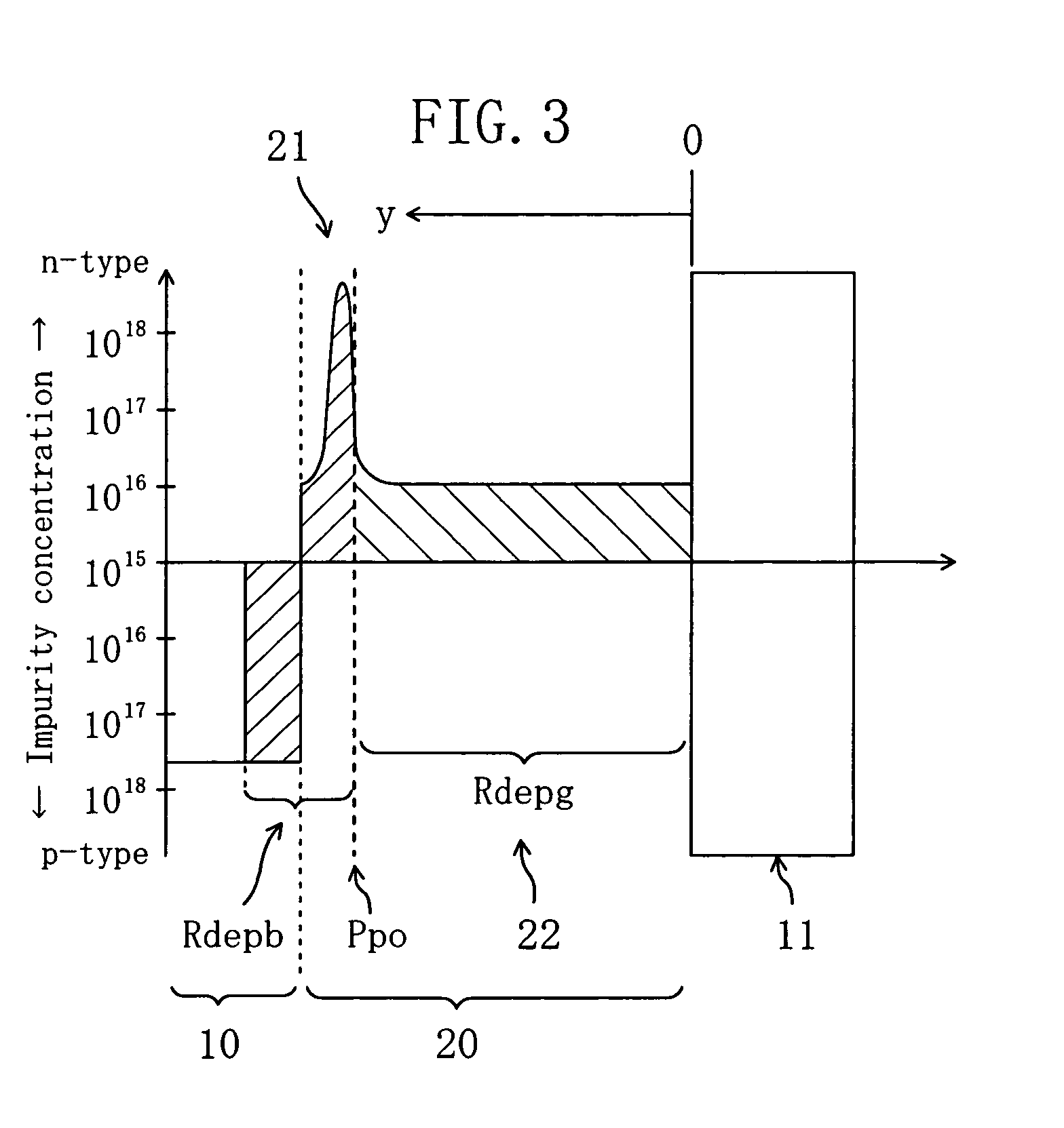
[0099]FIG. 8 shows relationship between the impurity concentrations of a channel layer and a pSiC layer, and depletion layers in a semiconductor device (SiC-MISFET (d-DACFET)) in accordance with a third embodiment of the present invention. As shown in FIG. 8, the d-DACFET of this embodiment includes in the channel layer, instead of the 6 doped layer 21 in the d-DACFET of the first embodiment shown in FIG. 1, a graded doped layer (high-concentration doped layer) in which impurity concentration decreases heading from its deeper portion toward its surface. The lower end of the graded doped layer is in contact with the pSiC layer. The impurity concentration of the deepest portion of the graded doped layer, which is about 5.0×10¹⁸·cm−3, decreases almost continuously tending toward the impurity concentration (about 1.×1016·cm−3) of the undoped layer. The graded doped layer has a thickness of about 10 nm.

[0100]In the d-DACFET of this embodiment, a depletion layer Rdepb that extends fr...


PUM


Abstract

A semiconductor device having an accumulation channel SiC-MISFET structure includes a p-type SiC layer 10 formed on an SiC substrate, an n-type channel layer 20, a gate insulating film 11, a gate electrode 12, and n-type source and drain layers 13a and 13b. The channel layer 20 includes an undoped layer 22 and a δ doped layer 21 which is formed in the vicinity of the lower end of the undoped layer 22. Since the channel layer 20 includes the high-concentration δ doped layer 21 in its deeper portion, the electric field in the surface region of the channel layer is weakened, thereby allowing the current driving force to increase.

Description

TECHNICAL FIELD[0001]The present invention relates to semiconductor devices having an accumulation channel MISFET structure, and more particularly relates to measures to obtain normally-off operation in power devices.BACKGROUND ART[0002]Since silicon carbide (hereinafter referred to as “SiC”) has a wide bandgap and high dielectric breakdown characteristics as compared with other semiconductor materials, applications in low-loss power devices are being anticipated. On an SiC layer, a relatively high quality silicon dioxide (SiO2) film is formed by thermal oxidation of the SiC. It is therefore presumably effective to adopt an insulated-gate structure for an SiC power conversion device.[0003]Nevertheless, a thermal oxide film, as a gate insulating film, formed on an SiC layer has many problems remaining to be overcome. For example, defects in a thermal oxide film cause high-density interface traps to be present in a region of the SiC layer in the vicinity of the interface with the insu...

Claims


Application Information

Patent Timeline
IPC IPC(8): H01L31/072H01L21/04H01L21/336H01L29/10H01L29/24H01L29/36H01L29/772H01L29/78
CPCH01L29/105H01L29/7838H01L29/7725H01L29/7828H01L29/66068H01L29/1608H01L29/365
Inventor YAMASHITA, KENYAKITABATAKE, MAKOTOKUSUMOTO, OSAMUTAKAHASHI, KUNIMASAUCHIDA, MASAOMIYANAGA, RYOKO
Owner PANASONIC CORP
Why Eureka
Try Eureka