Phase interpolator device and method

a phase interpolator and phase technology, applied in the field of data transceivers, can solve the problems of high power dissipation, deleterious electromagnetic radiative properties, oscillators used to generate such timing signals, etc., and achieve the effects of reducing power consumption, reducing frequency offset, and reducing power consumption

Inactive Publication Date: 2006-02-07
AVAGO TECH WIRELESS IP SINGAPORE PTE
View PDF49 Cites 31 Cited by
  • Summary
  • Abstract
  • Description
  • Claims
  • Application Information

AI Technical Summary

Benefits of technology

[0015]Each of the stage control signals may include a plurality of binary control subsignals. In this embodiment, the value of each stage control signal is the sum of the corresponding binary control signals. Each of these subsignals may be received by one of a plurality of scaling modules. As a result, the scaling factor of the respective reference stage increases with the value of the corresponding stage control signal.
[0031]In yet another embodiment, the present invention is directed to a communication device on an IC chip. The device is configured to receive multiple, analog serial data signals. The device comprises a master timing generator adapted to generate a master timing signal. The device also includes multiple receive-lanes, each configured to receive an associated one of the multiple serial data signals. Each receive-lane includes a phase interpolator adapted to produce a sampling signal having an interpolated phase, and a data path adapted to sample and quantize the associated serial data signal in accordance with the sampling signal. The device also includes an interpolator control module coupled to each receive-lane. The interpolator control module is adapted to cause the phase interpolator in each receive-lane to rotate the interpolated phase of the sampling signal in the receive-lane at a rate corresponding to a frequency offset between the sampling signal and the serial data signal associated with the receive-lane, so as to reduce the frequency offset between the sampling signal and the serial data signal.

Problems solved by technology

However, oscillators used to generate such timing signals have disadvantages, including typically large sizes, high power dissipation, and deleterious electromagnetic radiative properties (that is, the oscillators tend to radiate electromagnetic interference across the IC chip).
Also, oscillators used in communication devices often need to be tunable in both phase and frequency and in response to rapidly changing signals.
This requires complex oscillator circuitry.
Moreover, multiple oscillators on a common IC chip are subjected to undesired phenomena, such as phase and / or frequency injection locking, whereby one oscillator can deleteriously influence the operation of another oscillator.
As the received data signal rate increases into the multi-gigabit-per-second range, the difficulty in effectively controlling sampling processes in the receiver (such as controlling phase and frequency characteristics of the sampling signal) correspondingly increases.
For example, semiconductor circuits, such as complementary metal oxide semiconductor (CMOS) circuits, are often unable to operate at sufficiently high frequencies to optimally control the sampling processes.
For example, it becomes increasingly difficult at such high received signal data rates to provide sufficiently short time delays usable for controlling sampling phases of the sampling signal.

Method used


Image

  • Phase interpolator device and method
  • Phase interpolator device and method
  • Phase interpolator device and method

Examples


Embodiment Construction

I. Overview

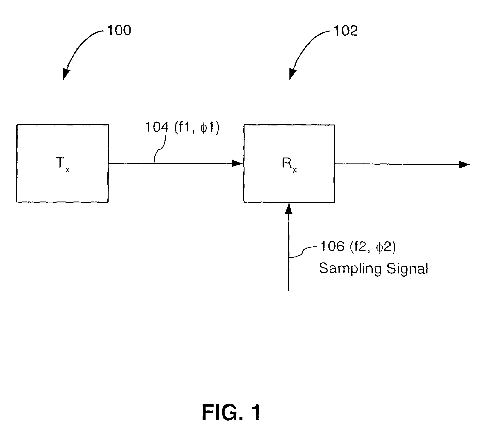
[0081]FIG. 1 is a block diagram of a simple communication system 100 including a transmitter 100 and a receiver 102. Transmitter 100 transmits a serial data signal 104 including, for example, a series of data symbols, to receiver 102. Serial data signal 104 has a frequency f1 (for example, a symbol baud rate f1) and a phase φ1 both related to a frequency and a phase of an oscillator (not shown) local to transmitter 100.

[0082]Receiver 102 samples serial data signal 104 (for example, symbols included in the serial data signal) to recover data from the serial data signal. Receiver 102 samples serial data signal at sample times established by a sampling signal 106 generated locally at receiver 102. Locally generated sampling signal 106 has a frequency f2 and a phase φ2.

[0083]To minimize errors in recovering the data from serial data signal 104, it is desirable that frequencies f2 and f1 match one another, and that phases φ1 and φ2 are aligned with one another, such that sampl...


PUM


Abstract

A high-speed serial data transceiver includes multiple receivers and transmitters for receiving and transmitting multiple analog, serial data signals at multi-gigabit-per-second data rates. Each receiver includes a timing recovery system for tracking a phase and a frequency of the serial data signal associated with the receiver. The timing recovery system includes a phase interpolator responsive to phase control signals and a set of reference signals having different predetermined phases. The phase interpolator derives a sampling signal, having an interpolated phase, to sample the serial data signal. The timing recovery system in each receiver independently phase-aligns and frequency synchronizes the sampling signal to the serial data signal associated with the receiver. A receiver can include multiple paths for sampling a received, serial data signal in accordance with multiple time-staggered sampling signals, each having an interpolated phase.

Description

CROSS-REFERENCES TO RELATED APPLICATIONS[0001]This application is a continuation of U.S. Non-Provisional application Ser. No. 10 / 346,210, filed Jan. 17, 2003, entitled “Phase Interpolator Device and Method,” which is a continuation of U.S. Non-Provisional application Ser. No. 09 / 844,266, filed Apr. 30, 2001, entitled “Phase Interpolator Device and Method,” which claims priority to U.S. Provisional Application No. 60 / 200,813, filed Apr. 28, 2000, entitled “High-Speed Serial Transceiver,” all of which are incorporated herein by reference in their entireties.BACKGROUND OF THE INVENTION[0002]1. Field of the Invention[0003]The present invention relates generally to data transceivers.[0004]2. Background Art[0005]A communication device including a transmitter and a receiver is known as a transceiver. Known transceivers can transmit and receive data signals. There are demands on such transceivers to transmit and receive such data signals with low error rates and at ever increasing data rate...

Claims


Application Information

Patent Timeline
Patent Type & Authority Patents(United States)
IPC IPC(8): H03H11/16H03L7/07H03L7/081H03L7/091H04L7/027H04L7/033H04L25/03
CPCH03L7/0814H03L7/091H04L7/0274H04L7/0041H04L25/03006H04L25/03885H04L7/0337H03L7/07H04L7/0025H04L2025/03477H04L2025/03617H03L7/0816
Inventor BUCHWALD, AARON W.WAKAYAMA, MYLESLE, MICHAELVAN ENGELEN, JURGENJIANG, XICHENGWANG, HUIBAUMER, HOWARD A.MADISETTI, AVANINDRA
Owner AVAGO TECH WIRELESS IP SINGAPORE PTE
Why Eureka
Try Eureka