Two-dimensional photonic crystal optical resonator and optical reflector using interference between point defects

a photonic crystal and optical resonator technology, applied in the field of optical resonators and optical reflectors, can solve the problems of deteriorating the light-extracting efficiency of optical resonators, increasing the size of devices, and not allowing light propagation,

Inactive Publication Date: 2006-02-07
JAPAN SCI & TECH CORP
View PDF7 Cites 9 Cited by
  • Summary
  • Abstract
  • Description
  • Claims
  • Application Information

AI Technical Summary

Benefits of technology

[0027]The low refractive index area may be created by embedding a material having a low refractive index in the body or just forming a hole in the body. In the latter case, the air constitutes the modified refractive index area. Practically, air is the material that has the lowest refractive index. Therefore, forming a hole is advantageous to increase the difference in the refractive index between the modified refractive index area and the body. This provides a high level of Q-factor as a resonator or reflector. Furthermore, forming a hole is easier than embedding a different material.
[0042]As described above, the optical resonator according to the second mode can be used as an optical reflector. When attention is paid to the entrance side of the traveling path of the progressive wave in the waveguide, the optical path difference 2L between the reflected light from defect 1 and that from defect 2 is equal to the wavelength multiplied by an integer, so that the two rays of reflected light intensify each other. This means that the light is efficiently reflected on the entrance side of the waveguide. This allows the optical resonator to be used as an optical filter that reflects a specific wavelength of light and does not allow it to pass through.
[0043]In the above-described optical reflector, another set of two point-like defects (or point-like defect pair) may be added to the opposite side of the waveguide. In this case, the distances in the width-direction of the waveguide may be slightly different, whereas the longitudinal position must be the same. In this case, the four point-like defects as a set constitute an optical reflector. This structure provides a higher efficiency of reflecting light than the optical reflector using two point-like defects as a set.
[0044]Use of the above-described optical reflector will strengthen the resonance occurring within the optical resonator of the second mode. In the second mode, the above-described set of two or four point-like defects are arranged at the locations of the defect 1 and defect 2, respectively. The set of two or four point-like defects reflects light more efficiently than a single point-like defect, so that the resonance occurring within the optical resonator of the second mode is strengthened and the light-extracting efficiency is improved.
[0045]In the first mode of two-dimensional photonic crystal optical resonator using interference between point defects according to the present invention, the reflected light and the transmitted light, which cause the deterioration in the light-extracting efficiency of conventional types of two-dimensional photonic crystal optical resonator using point defect, are suppressed. This leads to an increased intensity of light emitted from the point-like defect to the outside and improves the light-extracting efficiency.
[0047]Furthermore, the structure of the two-dimensional photonic crystal optical resonator using interference between point defects according to the second mode of the present invention can be used as an optical reflector. This enables the construction of a filter that blocks a specific wavelength of light included in the light propagated from one end and reflects the light.

Problems solved by technology

One of its particular features is that it has an energy region (called the photonic bandgap) that does not allow the propagation of light.
These methods, however, inevitably increase the size of the device, and are inefficient.
The presence of the reflected light and the transmitted light deteriorates the light-extracting efficiency of the optical resonator.

Method used


Image

  • Two-dimensional photonic crystal optical resonator and optical reflector using interference between point defects
  • Two-dimensional photonic crystal optical resonator and optical reflector using interference between point defects
  • Two-dimensional photonic crystal optical resonator and optical reflector using interference between point defects

Examples


Embodiment Construction

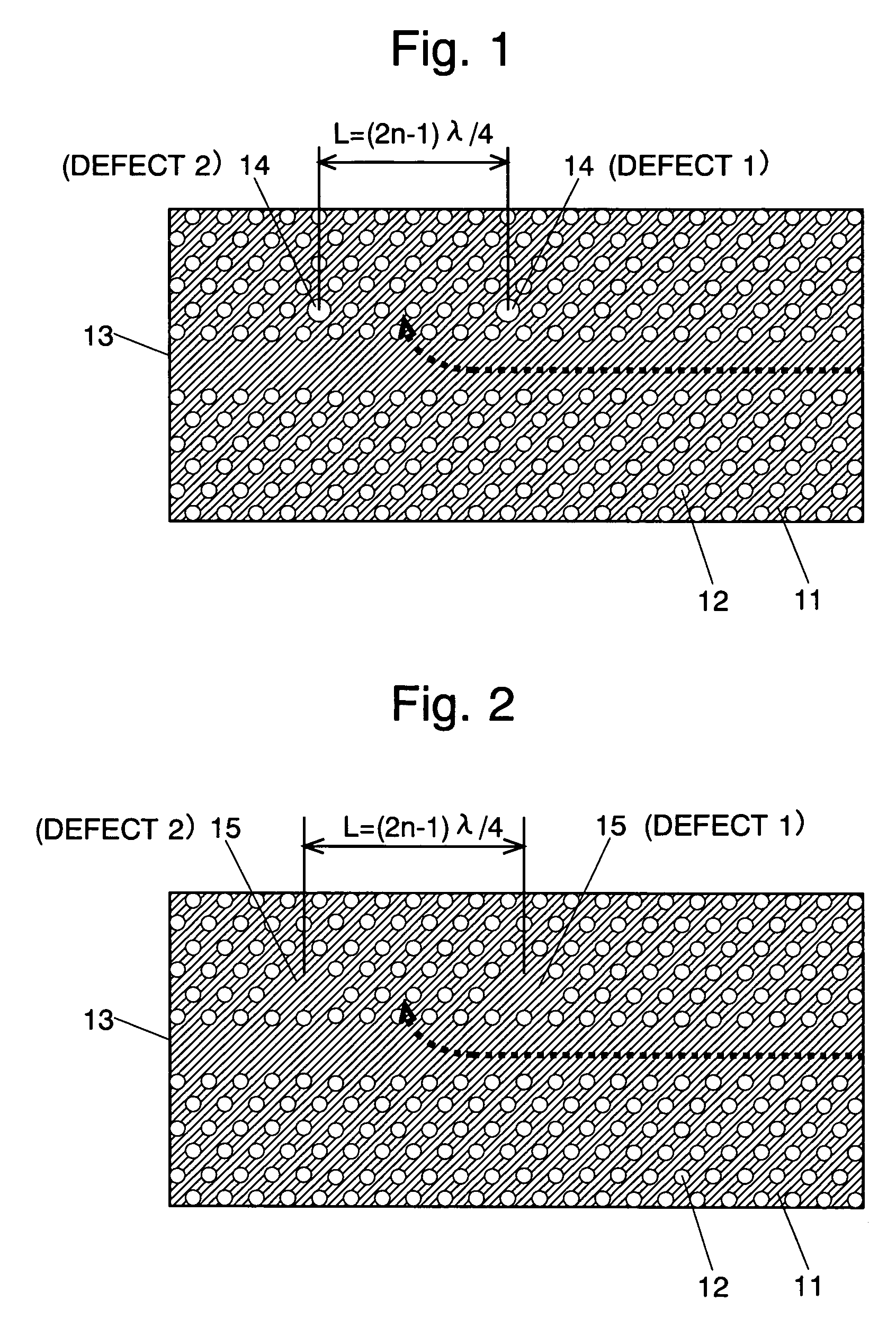
(1) Example of Structure According to First Mode

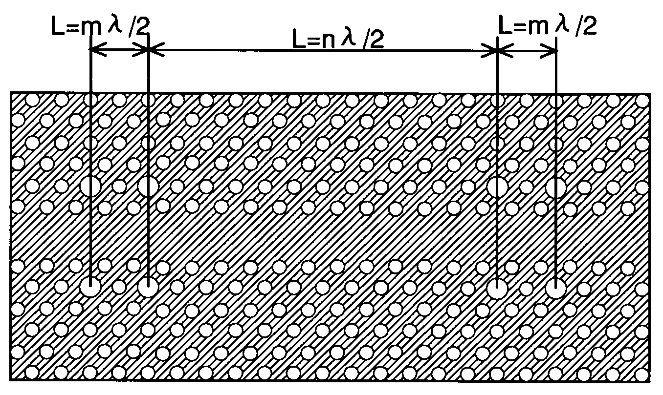
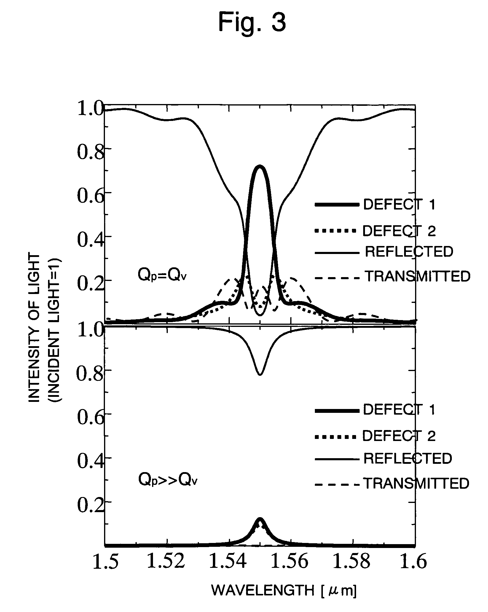
[0056]FIGS. 1 and 2 show an example of the structure of the two-dimensional photonic crystal optical resonator using interference between point defects according to the present invention. The plate-shaped object shown in FIGS. 1 and 2 is the slab (body) 11. When the infrared light of 1.5 μm waveband used in optical communications is considered, the slab 11 may be made from InGaAsP, which is transparent to that waveband.

[0057]On this slab 11, holes 12 are arranged at cycle a. These holes 12 are the modified refractive index areas, whereby a photonic bandgap is formed. FIGS. 1 and 2 show an example in which holes 12 are arranged in a triangular lattice pattern. It is possible to use other periodical arrangement patterns, such as a square lattice pattern.

[0058]The aforementioned Japanese Unexamined Patent Publication No. 2001-272555 teaches that the aforementioned waveband corresponds to the frequency range from 0.27c / a to 0.28c / a, where ...


PUM


Abstract

The present invention provides a two-dimensional photonic crystal optical resonator and reflector having high light-extracting efficiency. A two-dimensional photonic crystal consisting of a slab-shaped body is created by periodically arranging holes having a refractive index different from that of the body. A waveguide is formed by providing a linear zone where no hole is bored. Two acceptor type point defects are formed by enlarging two holes spaced apart from each other by a distance L in the longitudinal direction of the waveguide. An appropriate selection of the distance L suppresses or increases the reflection and transmission of light at the point defects, allowing an efficient extraction of light resonating at the point defects. This allows the body to be used as an optical resonator for producing a resonance of light between the two point defects or optical reflector for reflecting light at the two point defects.

Description

TECHNICAL FIELD[0001]The present invention relates to an optical resonator and an optical reflector that can be used, for example, as a light source for wavelength division multiplexing communication.BACKGROUND ART[0002]Recently, photonic crystals have been drawing attentions as a new optical device. A photonic crystal is an optical functional material having a periodic distribution of refractive index, which provides a band structure with respect to the energy of photons. One of its particular features is that it has an energy region (called the photonic bandgap) that does not allow the propagation of light.[0003]An example of the application fields of the photonic crystal is the optical communication. Recent optical communications use the wavelength division multiplexing (WDM) in place of a conventional method called the time division multiplexing (TDM). Wavelength division multiplexing is a communication method in which plural wavelengths of light, each carrying a different signa...

Claims


Application Information

Patent Timeline
Patent Type & Authority Patents(United States)
IPC IPC(8): G02B6/10G02B5/18G02B6/12G02B6/122G02B6/34H01S3/06H01S3/08H01S5/10
CPCB82Y20/00G02B6/12007G02B6/1225H01S5/10G02B6/122H01S5/105H01S5/11
Inventor NODA, SUSUMUASANO, TAKASHI
Owner JAPAN SCI & TECH CORP
Why Eureka
Try Eureka