Stacked gate flash memory device and method of fabricating the same

a technology of flash memory and gate array, which is applied in the direction of semiconductor devices, electrical devices, transistors, etc., can solve the problem of cost-effective fabrication of flash memory, and achieve the effect of high integration of memory cells

Active Publication Date: 2006-02-14
NAN YA TECH
View PDF4 Cites 24 Cited by
  • Summary
  • Abstract
  • Description
  • Claims
  • Application Information

AI Technical Summary

Benefits of technology

[0008]Accordingly, an object of the invention is to provide a stacked gate flash memory device that can achieve high integration of memory cells thereof.
[0009]Another object of the invention is to provide a method of fabricating a stacked gate flash memory device, wherein the size of memory cells thereof can be reduced and the coupling ratio of the control gate to the floating gate can be also increased.
[0012]In the present invention, the trench-type stacked gate flash memory device disposed in cell trenches within a substrate can achieve higher integration of memory cell capacity than that in the Prior Art.
[0013]Moreover, the control gate in the invention can be L-shaped or reverse L-shaped (), the overlapping areas between the floating gate and the control gate can be larger and a higher coupling ratio to the control gate can be obtained.
[0014]In addition, most of the fabricating processes in the invention are self-aligned and additional lithography processes and number of masks for the whole fabricating process can be reduced. The complexity of fabrication is reduced and can be easily achieved. The higher coupling ratio by the memory cells also provided a lower operating voltage thereof.
[0015]Furthermore, most patterns of the masks for fabricating the stacked gate flash memory device are rectangular and can be easily fabricated. The costs of mask fabrication can be reduced and resolution limitations by the photolithography tools can be reduced.

Problems solved by technology

Furthermore, fabricating flash memory is cost effective.

Method used


Image

  • Stacked gate flash memory device and method of fabricating the same
  • Stacked gate flash memory device and method of fabricating the same
  • Stacked gate flash memory device and method of fabricating the same

Examples


Embodiment Construction

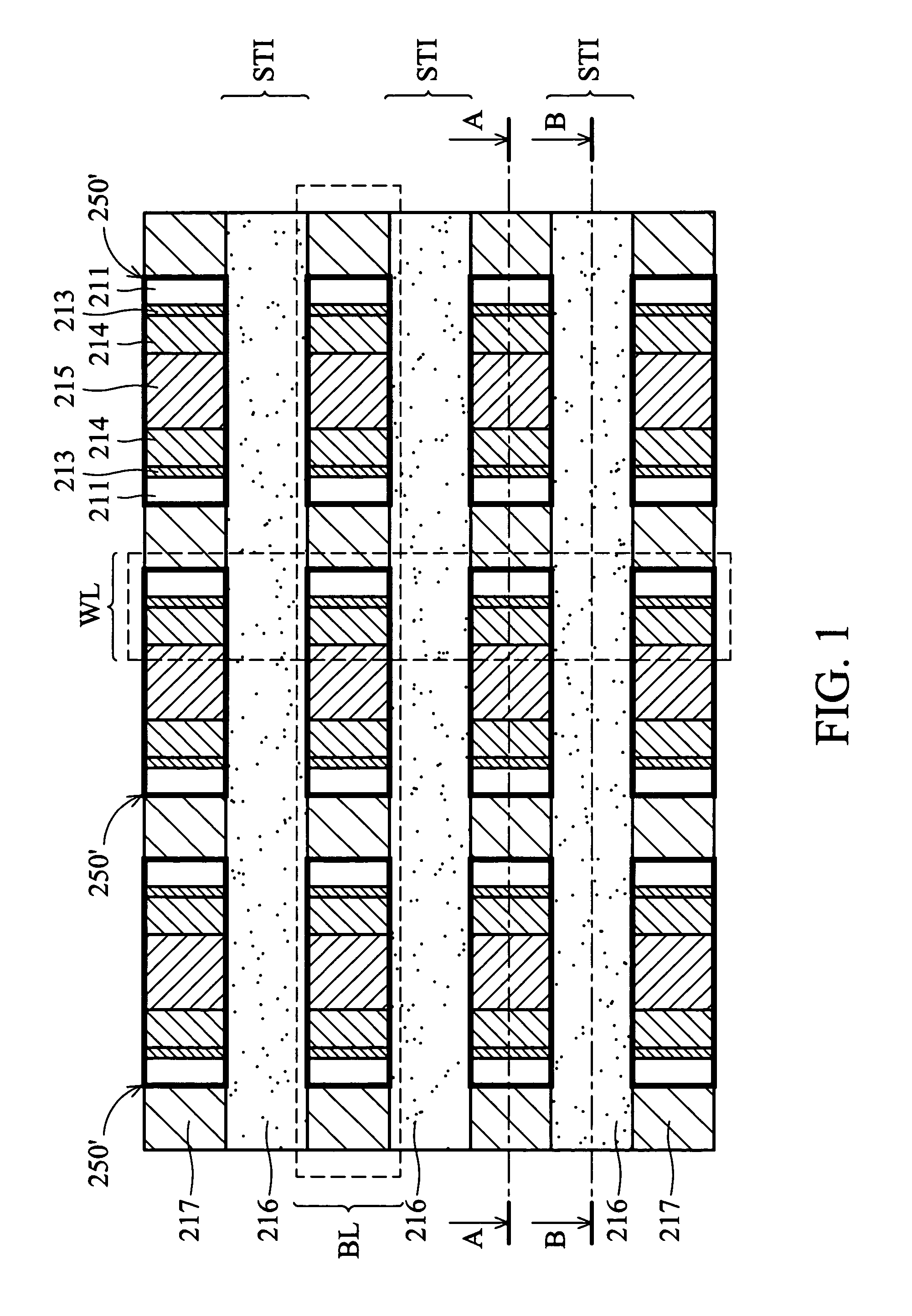
[0022]The present invention provides a stacked gate flash memory device that meets the demand for increased capacity of memory cells. In FIG. 1, a top view of the stacked gate flash memory device in accordance with the present invention is shown. Each memory cell is disposed in the cell trenches (referring to trench 250′) along the A˜A′ phantom line, between two shallow isolation trench (referring to STI) regions along the B˜B′ phantom line.

[0023]FIGS. 3a˜3j and FIGS. 4a˜4j respectively illustrate the cross-sections of a fabricating process along lines A˜A′ and lines B˜B′ according to an embodiment of the present invention. Moreover, FIGS. 2a˜2d also illustrate corresponding top views of the fabricating process.

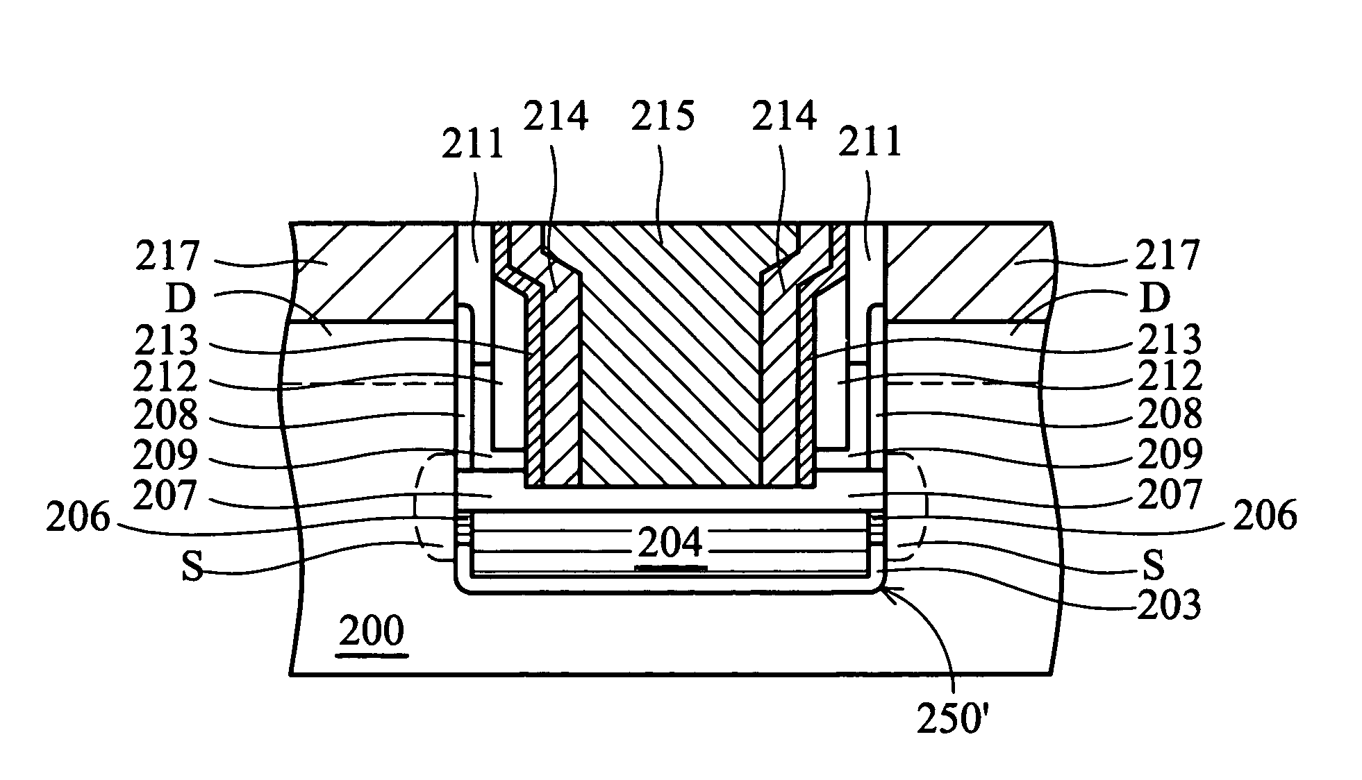
[0024]First, FIG. 3j illustrates a cross-section of the stacked gate flash memory device in accordance with the present invention. A cell of the memory device comprises a substrate 200 having a trench 250′ therein. A conductive layer composed of a source material line layer 2...


PUM


Abstract

A stacked gate flash memory device and method of fabricating the same. A cell of the stacked gate flash memory device is disposed in a cell trench within a substrate to achieve higher integration of memory cells.

Description

BACKGROUND OF THE INVENTION[0001]1. Field of the Invention[0002]The present invention relates to a semiconductor device and method of fabricating the same. More particularly, it relates to a stacked gate flash memory device that can achieve high memory cell capacity.[0003]2. Description of the Related Art[0004]Complementary metal oxide semiconductor (CMOS) memory is generally categorized into two groups: random access memory (RAM) and read only memory (ROM). RAM is a volatile memory, wherein the stored data is erased when power is turned off. On the contrary, turning off power does not affect the stored data in a ROM.[0005]In the past few years, market share of ROM has been continuously expanding, and the type attracting the most attention has been flash memory. The fact that a single memory cell is electrically programmable and multiple memory cell blocks are electrically erasable allows flexible and convenient application, superior to electrically programmable read only memory (EP...

Claims


Application Information

Patent Timeline
Patent Type & Authority Patents(United States)
IPC IPC(8): H01L21/336H01L21/8247H01L27/115H01L29/423H01L29/788
CPCH01L27/115H01L29/7883H01L29/42336H01L27/11556H10B69/00H10B41/27
Inventor LIN, CHI-HUI
Owner NAN YA TECH
Why Eureka
Try Eureka