Method for manufacturing shallow trench isolation in semiconductor device

a semiconductor device and trench isolation technology, applied in semiconductor/solid-state device manufacturing, basic electric elements, electric devices, etc., can solve the problems of reducing the design rule, deteriorating field oxide (fox), and rarely using locos technique to form, so as to improve the gap-filling property

Inactive Publication Date: 2006-02-14
SK HYNIX INC
View PDF6 Cites 23 Cited by
  • Summary
  • Abstract
  • Description
  • Claims
  • Application Information

AI Technical Summary

Benefits of technology

[0016]It is, therefore, an object of the present invention to provide a method for manufacturing a shallow trench isolation (STI) in a semiconductor device with an enhanced gap-fill property and without a detrimental effect of fluorine by employing a two-stage thermal process.

Problems solved by technology

The LOCOS technique, however, has several drawbacks that a field oxide (FOX) is deteriorated with a decrease of a design rule and further, a bird's beak structure encroached into an active area of the device.
Thus, the LOCOS technique is rarely employed to form the isolation region as the device becomes micro-miniaturized in nowadays.
However, there is still a limitation to apply the conventional He-based HDP oxide for forming the STI in the micro-miniaturized semiconductor device.
Therefore, in case of using the He-based HDP oxide for the STI, there are inevitably happened micro-voids therein.
But, since there exists a fluorine (F) in the NF3-based HDP oxide layer 122, the fluorine has a detrimental effect on a gate oxide during a post thermal process.
Therefore, it is difficult to expect a reliable semiconductor device in the long run.

Method used


Image

  • Method for manufacturing shallow trench isolation in semiconductor device
  • Method for manufacturing shallow trench isolation in semiconductor device
  • Method for manufacturing shallow trench isolation in semiconductor device

Examples


Embodiment Construction

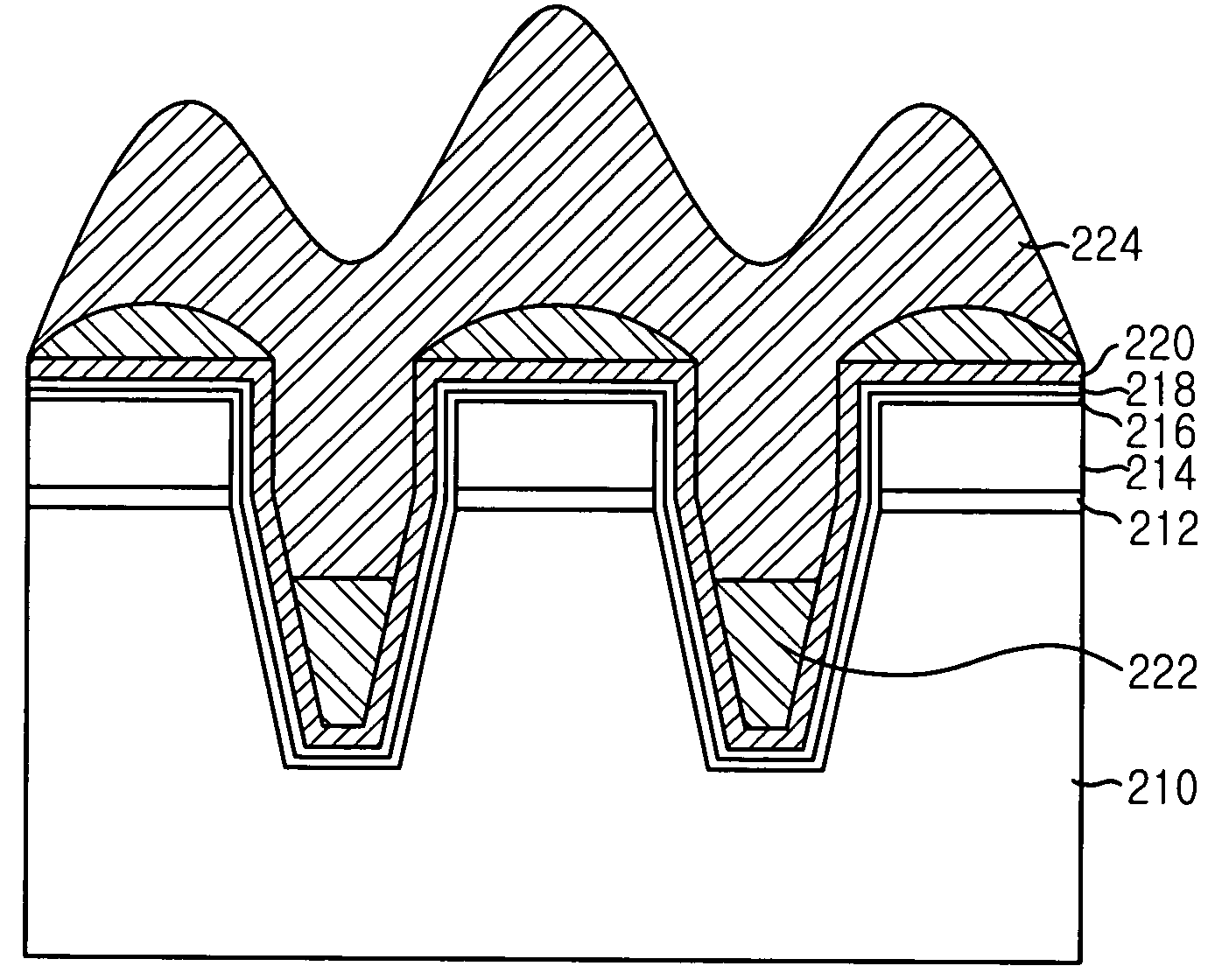
[0023]There are provided in FIGS. 2A to 2C and FIGS. 3A and 3B cross sectional views setting forth a method for manufacturing a shallow trench isolation (STI) in a semiconductor device in accordance with a preferred embodiment of the present invention. It should be noted that like parts appearing in FIGS. 2A to 2C and FIGS. 3A and 3B are represented by like reference numerals.

[0024]Referring to FIG. 2A, a process for manufacturing the STI in the semiconductor device begins with preparing a semiconductor substrate 210 obtained by a predetermined process. Afterward, a pad oxide layer and a pad nitride layer are formed on the semiconductor substrate 210 in sequence. Then, photoresist masks (not shown) are formed on predetermined locations of a top face of the pad nitride layer. Thereafter, the pad nitride layer and the pad oxide layer are patterned into a first predetermined configuration by using the photoresist masks as mask patterns till a top face of the semiconductor substrate 210...


PUM


Abstract

The method for manufacturing a shallow trench isolation (STI) in a semiconductor device with an enhanced gap-fill property and without a detrimental effect of fluorine by introducing a two-stage thermal process. The method includes steps of: preparing a semiconductor substrate obtained by a predetermined process on which a pad oxide and a pad nitride are formed on predetermined locations thereof; forming a trench structure in the semiconductor substrate; forming a hydrogen (H2)-based high density plasma (HDP) oxide layer over a first resultant structure; forming a nitrogen trifluoride (NF3)-based HDP oxide layer into the trench structure with a predetermined depth; carrying out a two-stage thermal process for removing fluorine in the NF3-based HDP oxide layer; and forming a helium (He)-based HDP oxide layer over a second resultant structure.

Description

FIELD OF THE INVENTION[0001]The present invention relates to a method for manufacturing a semiconductor device; and, more particularly, to a method for manufacturing a shallow trench isolation (STI) for use in a highly integrated semiconductor device with an enhanced gap-fill property and simultaneously, without a detrimental impact of fluorine by employing a two-stage thermal process.DESCRIPTION OF THE PRIOR ART[0002]As is well known, in a semiconductor device, there is formed an isolation region for electrically isolating elements from each other. In order to form the isolation region, various techniques have been employed such as a local oxidation of silicon (LOCOS) which uses a thermal oxide or a shallow trench isolation (STI) technique which is suitable for a highly integrated semiconductor device.[0003]The LOCOS technique, however, has several drawbacks that a field oxide (FOX) is deteriorated with a decrease of a design rule and further, a bird's beak structure encroached int...

Claims


Application Information

Patent Timeline
Patent Type & Authority Patents(United States)
IPC IPC(8): H01L21/76H01L21/469H01L21/762
CPCH01L21/76224H01L21/76
Inventor KIM, JAE-HONG
Owner SK HYNIX INC
Why Eureka
Try Eureka