Thermal flux processing by scanning

a technology of flux processing and scanning, applied in the field of thermal processing, can solve the problem of not being able to meet the rate requirements, reduce the total radiated power requirement, and shorten the annealing time

Inactive Publication Date: 2006-02-28
APPLIED MATERIALS INC
View PDF42 Cites 100 Cited by
  • Summary
  • Abstract
  • Description
  • Claims
  • Application Information

AI Technical Summary

Benefits of technology

[0016]Therefore, the present invention heats only a small portion of the surface of the substrate at any given moment, thereby achieving very short annealing times. This reduces the total radiated power requirement. In fact, an energy density of 150 kW / cm2 is achievable on a 300 mm wafer from a 5 kW radiation source. In addition, process control is achieved by modulating scan speed rather than lamp power, thereby simplifying the control of the apparatus. This allows for highly local heating without generating defects.

Problems solved by technology

However, these ramp rates are not too high as to prevent some thermal diffusion from occurring, as limited thermal diffusion is extremely useful for homogenizing the exposure.

Method used


Image

  • Thermal flux processing by scanning
  • Thermal flux processing by scanning
  • Thermal flux processing by scanning

Examples


Embodiment Construction

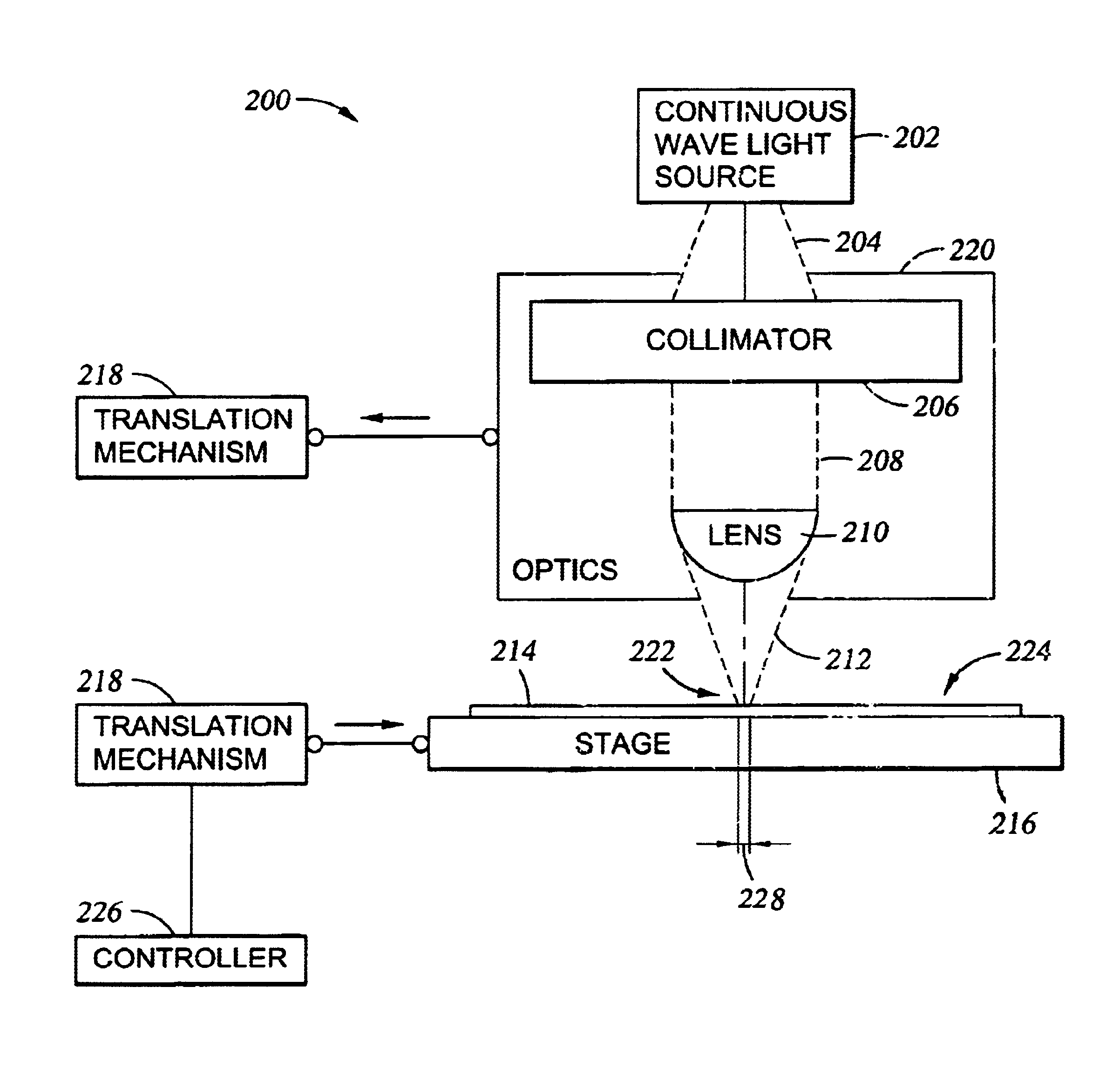
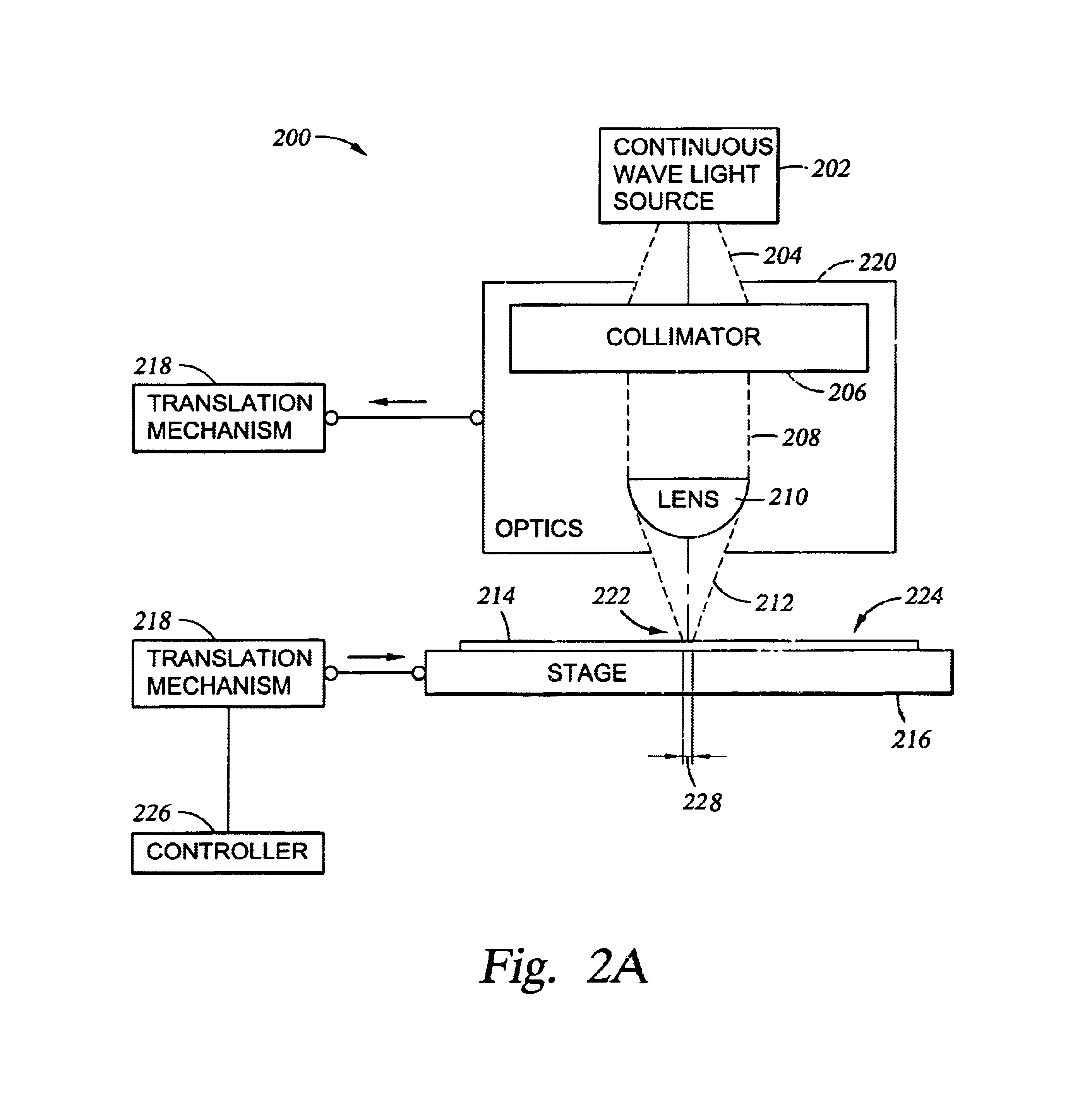
[0026]FIG. 2A is a side view of an apparatus 200 for thermally processing a semiconductor substrate, according to an embodiment of the invention. For the practice of the invention, the preferred thermal process is annealing and annealing will be described throughout the remainder of the Figures. The apparatus 200 comprises a continuous wave electromagnetic radiation source 202, a stage 216 configured to receive a semiconductor substrate 214 thereon, and optics 220 disposed between the continuous wave electromagnetic radiation source 202 and the stage 216.

[0027]In a preferred embodiment, the semiconductor substrate 214 is any substrate having high thermal conductivity, such as a single crystal silicon substrate, silicon on insulator (SOI), Silicon Germanium or alloys thereof, or the like. It should be appreciated that the semiconductor substrate 214 is not a glass or quartz substrate with a silicon layer thereon, as used for manufacturing thin film transistors (TFT). Thermal flux pro...


PUM

PropertyMeasurementUnit
poweraaaaaaaaaa
poweraaaaaaaaaa
poweraaaaaaaaaa

Abstract

The thermal flux processing device includes a continuous wave electromagnetic radiation source, a stage, optics, and a translation mechanism. The continuous wave electromagnetic radiation source is preferably a diode / s. The stage is configured to receive a semiconductor substrate thereon. The optics are preferably disposed between the continuous wave electromagnetic radiation source and the stage. Also, the optics are configured to focus continuous wave electromagnetic radiation from the continuous wave electromagnetic radiation source into a line of continuous wave electromagnetic radiation on an upper surface of the semiconductor substrate. A length of the line of continuous wave electromagnetic radiation extends across an entire width of the semiconductor substrate. The translation mechanism is configured to translate the stage and the line of continuous wave electromagnetic radiation relative to one another, and preferably includes a chuck for securely grasping the substrate. A method for thermally processing a semiconductor substrate is also provided.

Description

BACKGROUND OF THE INVENTION[0001]1. Field of the Invention[0002]The invention relates generally to thermal processing. More particularly, the invention is directed to an apparatus and method for thermally processing a semiconductor substrate by scanning the substrate with a line of radiation.[0003]2. Description of Related Art[0004]The integrated circuit (IC) market is continually demanding greater memory capacity, faster switching speeds, and smaller feature sizes. One of the major steps the industry has taken to address these demands is to change from batch processing silicon wafers in large furnaces to single wafer processing in a small chamber.[0005]During such single wafer processing the wafer is typically heated to high temperatures so that various chemical and physical reactions can take place in multiple IC devices defined in the wafer. Of particular interest, favorable electrical performance of the IC devices requires implanted regions to be annealed. Annealing recreates a ...

Claims


Application Information

Patent Timeline
Patent Type & Authority Patents(United States)
IPC IPC(8): B23K26/00B23K26/03B23K26/06B23K26/08B23K26/12B23K26/34C23C8/00C23C8/10C23C8/22C23C16/04C23C16/48H01L21/20
CPCB23K26/03B23K26/3266B23K26/0665B23K26/0807B23K26/083B23K26/0838B23K26/123B23K26/34C23C8/00C23C8/10C23C8/22C23C16/047C23C16/481H01L21/2026B23K26/0652B23K26/0643B23K2201/40B23K26/082B23K26/32B23K2101/40B23K2103/50H01L21/02683H01L21/02678H01L21/02422H01L21/0242H01L21/02381H01L21/02691H01L21/0262H01L21/02532
Inventor JENNINGS, DEAN
Owner APPLIED MATERIALS INC
Why Eureka
Try Eureka